
Page 285 - Rashid, Power Electronics Handbook
P. 285
15 Resonant and Soft-Switching Converters 275
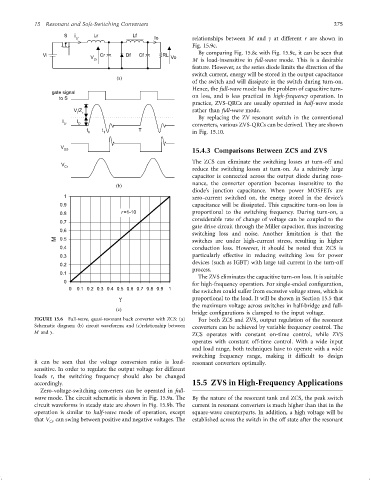
S i Lr Lr Lf Io relationships between M and g at different r are shown in
Fig. 15.9c.
By comparing Fig. 15.8c with Fig. 15.9c, it can be seen that
Vi Cr Df Cf RL
V Vo
Cr M is load-insensitive in full-wave mode. This is a desirable
feature. However, as the series diode limits the direction of the
switch current, energy will be stored in the output capacitance
(a)
of the switch and will dissipate in the switch during turn-on.
Hence, the full-wave mode has the problem of capacitive turn-
gate signal
to S on loss, and is less practical in high-frequency operation. In
practice, ZVS-QRCs are usually operated in half-wave mode
V/Z rather than full-wave mode.
i r
By replacing the ZV resonant switch in the conventional
I I
Lr O converters, various ZVS-QRCs can be derived. They are shown
t t T
0 1 in Fig. 15.10.
V
DS 15.4.3 Comparisons Between ZCS and ZVS
The ZCS can eliminate the switching losses at turn-off and
V
Cr
reduce the switching losses at turn-on. As a relatively large
capacitor is connected across the output diode during reso-
nance, the converter operation becomes insensitive to the
(b)
diode's junction capacitance. When power MOSFETs are
1 zero-current switched on, the energy stored in the device's
0.9 capacitance will be dissipated. This capacitive turn-on loss is
0.8 r =1-10 proportional to the switching frequency. During turn-on, a
considerable rate of change of voltage can be coupled to the
0.7
gate drive circuit through the Miller capacitor, thus increasing
0.6
switching loss and noise. Another limitation is that the
M 0.5 switches are under high-current stress, resulting in higher
0.4 conduction loss. However, it should be noted that ZCS is
0.3 particularly effective in reducing switching loss for power
devices (such as IGBT) with large tail current in the turn-off
0.2
process.
0.1
The ZVS eliminates the capacitive turn-on loss. It is suitable
0
for high-frequency operation. For single-ended con®guration,
0 0.1 0.2 0.3 0.4 0.5 0.6 0.7 0.8 0.9 1
the switches could suffer from excessive voltage stress, which is
g proportional to the load. It will be shown in Section 15.5 that
the maximum voltage across switches in half-bridge and full-
(c)
bridge con®gurations is clamped to the input voltage.
FIGURE 15.6 Full-wave, quasi-resonant buck converter with ZCS: (a) For both ZCS and ZVS, output regulation of the resonant
Schematic diagram; (b) circuit waveforms; and (c)relationship between converters can be achieved by variable frequency control. The
M and g.
ZCS operates with constant on-time control, while ZVS
operates with constant off-time control. With a wide input
and load range, both techniques have to operate with a wide
switching frequency range, making it dif®cult to design
it can be seen that the voltage conversion ratio is load- resonant converters optimally.
sensitive. In order to regulate the output voltage for different
loads r, the switching frequency should also be changed
accordingly. 15.5 ZVS in High-Frequency Applications
Zero-voltage-switching converters can be operated in full-
wave mode. The circuit schematic is shown in Fig. 15.9a. The By the nature of the resonant tank and ZCS, the peak switch
circuit waveforms in steady state are shown in Fig. 15.9b. The current in resonant converters is much higher than that in the
operation is similar to half-wave mode of operation, except square-wave counterparts. In addition, a high voltage will be
that V can swing between positive and negative voltages. The established across the switch in the off state after the resonant
Cr