
Page 292 - Rashid, Power Electronics Handbook
P. 292
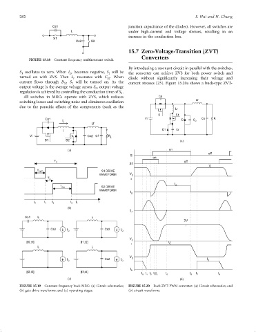
282                                                                                  S. Hui and H. Chung

                               Cs1                                  junction capacitance of the diodes). However, all switches are
                                        L                           under high-current and voltage stresses, resulting in an
                                                                    increase in the conduction loss.
                                S1
                                           Cs2    S2
                                                                    15.7 Zero-Voltage-Transition (ZVT)
                                                                          Converters
                    FIGURE 15.18  Constant frequency multiresonant switch.

                                                                    By introducing a resonant circuit in parallel with the switches,
               S oscillates to zero. When I Lr  becomes negative, S will be  the converter can achieve ZVS for both power switch and
                                                          1
                1
               turned on with ZVS. Then L resonates with C . When   diode without signi®cantly increasing their voltage and
                                         r
                                                          S2
               current ¯ows through D S2  S will be turned on. As the  current stresses [23]. Figure 15.20a shows a buck-type ZVT-
                                         2
               output voltage is the average voltage across S , output voltage
                                                    2
               regulation is achieved by controlling the conduction time of S :
                                                                2
                 All switches in MRCs operate with ZVS, which reduces              Cd
                                                                                                     Lf
               switching losses and switching noise and eliminates oscillation
               due to the parasitic effects of the components (such as the
                                                                                           Lr
                                                                                  S        S1
                            Cs1                                             Vi                D    C   Co    R
                                    i                                                               D
                                     L
                                                  Lf
                                    L                                               D1     Cr
                    Vi                          Cs2  Cf   R
                                                           L
                            S1        S2                                                     (a)
                                       (a)                                              on
                                                                                                           off
                                                                     S
                                                                                on
                                T                                                              off
                                 S
                                                                    S1
                                                                                                           V i
                        T                              S1 DRIVE
                         OFF
                                                      WAVEFORM       V D
                             T
                              D                                      S
                                                                                          I
                                   T                   S2 DRIVE                            O
                                    ON
                                                      WAVEFORM
                                                                     I
                                                                     S
                      t    t   t        t  t          t
                       0    1   2       3  4
                                       (b)
                                                                     I
                                                                     Lr
                  Cs1   L                         L
                                                                                               2V
                                                                                                i
                              Cs2     I                  Cs2    I
                                       O                         O
                                                                     V
                   [t0,t1]                   [t1,t2]                  C                V
                                                                     r                  i
                        L                         L
                                                                     V
                                      I                  Cs2    I     D                                   I
                                       O                         O                                        O
                                                                     I
                   [t2,t3]                   [t3,t4]                 D    t  t  t  t t  t         t  t         t
                                                                           0  1  2  3  4  5       6  7          0
                                       (c)                                                   (b)
               FIGURE 15.19  Constant frequency buck MRC: (a) Circuit schematics;  FIGURE 15.20  Buck ZVT-PWM converter: (a) Circuit schematics; and
               (b) gate drive waveforms; and (c) operating stages.  (b) circuit waveforms.