Page 296 - Rashid, Power Electronics Handbook
P. 296

286                                                                                  S. Hui and H. Chung

                   i                                                       5
                    Lr
                            v
                             Cr
                                                                           4
                 I
                  O
                                                                           3
                  0                                           w t                                 r=3
                                                               0
                                                                         M
                                                                           2
                                                                                              2
                          D
                      T
                       1                                                   1
                          1
                                                                                            0.8           1.27
                   t  t  t  t t  t
                   0  1   2  3 4  5                                                                       1
                                        (a)                                0
                                                                            0                  1                 2
                                                                                               g
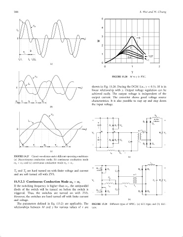
                              v                                                   FIGURE 15.28  M vs g in PRC.
                              Cr
                         i
                         Lr
                                                                    shown in Fig. 15.28. During the DCM (i.e., g < 0:5), M is in
                 0                                          w t
                                                             0
                                                                    linear relationship with g. Output voltage regulation can be
                                                                    achieved easily. The output voltage is independent of the
                                                                    output current. The converter shows good voltage source
                                                                    characteristics. It is also possible to step up and step down
                 D  T    D    T   D
                  2  1    1    2   2
                                                                    the input voltage.
                                        (b)
                                        v
                                         Cr                                                                    L
                                                                                                               d
                                                                                                              dc link
                         i                                          +                                                +
                         Lr                                                                            D      inductor
                                                                        +                              1     D
                                                                        E       S  D   C                      3
                                                                                 1  1   n
                                                                        -
                 0                                             w t
                                                                0                                  n:1 i
                                                                          B        A                  rect.in
                                                                    V                                             R  V
                                                                     s                                             L  o
                                                                        +
                                                                        E       S  D   C
                                                                                 2  2   n
                                                                        -                    C t    T 1  D   D
                     D      T       D      T      D                  -                                 2      4      -
                      1      1       2      2       1
                                        (c)
                                                                                L      C  i
                                                                                 s      s
               FIGURE 15.27  Circuit waveforms under different operating conditions:         (a)
               (a) Discontinuous conduction mode; (b) continuous conduction mode
               o S < o r ; and (c) continuous conduction mode o S > o r .                                   L o
                                                                    +  Q       D                   D      D          +
               T and T are hard turned on with ®nite voltage and current  1     1   C 1             5      7
                       2
                 1
               and are soft turned off with ZVS.                                                n:1
                                                                               C
                                                                                p
                                                                    V                                        C    R  V
               15.9.2.3 Continuous Conduction Mode v > v    r        s                                        L    L  o
                                                       S
               If the switching frequency is higher than o , the antiparallel  L p        L s   T 1
                                                   r
               diode of the switch will be turned on before the switch is  Q 2  D   C 2            D      D
               triggered. Thus, the switches are turned on with ZVS.  -         2                   6      8         -
               However, the switches are hard turned off with ®nite current
               and voltage.                                                                  (b)
                 The parameters de®ned in Eq. (15.2) are applicable. The  FIGURE 15.29  Different types of SPRC.: (a) LCC-type; and (b) LLC-
               relationships between M and g for various values of r are  type.
   291   292   293   294   295   296   297   298   299   300   301