Page 299 - Rashid, Power Electronics Handbook
P. 299

15  Resonant and Soft-Switching Converters                                                          289

                 DELCD. Separate delays are provided for the two half-bridges               L              D
                                                                                             F              F
                 to accommodate differences in resonant capacitor charging
                 currents. The delay in each set is approximated by        1-phase                 C r   L r    C
                                                                          AC supply           Q2   Ds2    SW1     F
                                  25   10 ÿ12 R DEL
                        t DELAY  ¼                 þ 25 ns     ð15:5Þ
                               0:75ðV CS  ÿ V ADS Þþ 0:5
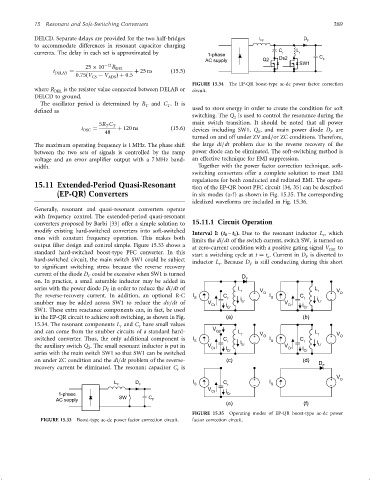
                                                                      FIGURE 15.34  The EP-QR boost-type ac-dc power factor correction
                 where R DEL  is the resistor value connected between DELAB or  circuit.
                 DELCD to ground.
                   The oscillator period is determined by R  and C .It is
                                                      T       T
                 de®ned as                                            used to store energy in order to create the condition for soft
                                                                      switching. The Q is used to control the resonance during the
                                                                                    2
                                       5R C T                         main switch transition. It should be noted that all power
                                         T
                                 t OSC  ¼    þ 120 ns          ð15:6Þ  devices including SW1, Q , and main power diode D are
                                         48                                                 1                       F
                                                                      turned on and off under ZV and=or ZC conditions. Therefore,
                 The maximum operating frequency is 1 MHz. The phase shift  the large di=dt problem due to the reverse recovery of the
                 between the two sets of signals is controlled by the ramp  power diode can be eliminated. The soft-switching method is
                 voltage and an error ampli®er output with a 7 MHz band-  an effective technique for EMI suppression.
                 width.                                                 Together with the power factor correction technique, soft-
                                                                      switching converters offer a complete solution to meet EMI
                                                                      regulations for both conducted and radiated EMI. The opera-
                 15.11 Extended-Period Quasi-Resonant                 tion of the EP-QR boost PFC circuit [34, 35] can be described
                         (EP-QR) Converters                           in six modes (a-f) as shown in Fig. 15.35. The corresponding
                                                                      idealized waveforms are included in Fig. 15.36.
                 Generally, resonant and quasi-resonant converters operate
                 with frequency control. The extended-period quasi-resonant
                 converters proposed by Barbi [33] offer a simple solution to  15.11.1 Circuit Operation
                 modify existing hard-switched converters into soft-switched
                                                                      Interval I: (t 0 ± t 1 ). Due to the resonant inductor L , which
                                                                                                                 r
                 ones with constant frequency operation. This makes both
                                                                      limits the di=dt of the switch current, switch SW is turned on
                                                                                                             1
                 output ®lter design and control simple. Figure 15.33 shows a  at zero-current condition with a positive gating signal V  to
                                                                                                                    GS1
                 standard hard-switched boost-type PFC converter. In this  start a switching cycle at t ¼ t . Current in D is diverted to
                                                                                                            F
                                                                                               o
                 hard-switched circuit, the main switch SW1 could be subject  inductor L . Because D is still conducting during this short
                 to signi®cant switching stress because the reverse recovery   r         F
                 current of the diode D could be excessive when SW1 is turned
                                   F                                                   D
                 on. In practice, a small saturable inductor may be added in            F
                 series with the power diode D in order to reduce the di=dt of       L                         L
                                         F                                            r      V                  r     V
                 the reverse-recovery current. In addition, an optional R-C  I  C             O  I        C            O
                                                                       S          r   i         S          r    i
                 snubber may be added across SW1 to reduce the dv=dt of    V          Lr             V          Lr
                                                                            Cr   i Cr                 Cr   i Cr
                 SW1. These extra reactance components can, in fact, be used
                 in the EP-QR circuit to achieve soft switching, as shown in Fig.  (a)                     (b)
                 15.34. The resonant components L and C have small values
                                                    r
                                              r
                 and can come from the snubber circuits of a standard hard-  V G2    L                         L
                                                                                      r      V O                r     V O
                 switched converter. Thus, the only additional component is  I  C               I         C
                                                                       S          r   i         S          r    i
                 the auxiliary switch Q . The small resonant inductor is put in  V Cr  i  Lr         V Cr  i    Lr
                                   2
                 series with the main switch SW1 so that SW1 can be switched      Cr                       Cr
                 on under ZC condition and the di=dt problem of the reverse-     (c)                       (d)
                                                                                                                D F
                 recovery current be eliminated. The resonant capacitor C is
                                                                 r
                                                                                                                      V O
                                            L      D                  I         C               I
                                             F      F                  S          r             S
                                                                           V Cr
                         1-phase                                                 i Cr
                         AC supply            SW       C F
                                                                                 (e)                       (f)
                                                                      FIGURE 15.35  Operating modes of EP-QR boost-type ac-dc power
                    FIGURE 15.33  Boost-type ac-dc power factor correction circuit.  factor correction circuit.
   294   295   296   297   298   299   300   301   302   303   304