
Page 300 - Rashid, Power Electronics Handbook
P. 300
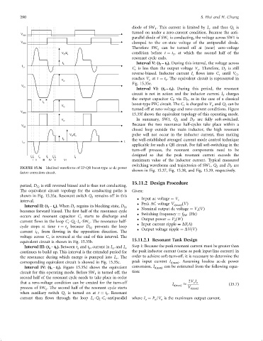
290 S. Hui and H. Chung
diode of SW . This current is limited by L and thus Q is
2
1
r
turned on under a zero-current condition. Because the anti-
V
GS1
parallel diode of SW is conducting, the voltage across SW1 is
1
V
GS2 clamped to the on-state voltage of the antiparallel diode.
Therefore SW 1 can be turned off at (near) zero-voltage
V /Z condition before t ¼ t , at which the second half of the
O n 2
resonant cycle ends.
I Interval V: (t 2 ± t 3 ). During this interval, the voltage across
S
i
Lr
C is less than the output voltage V . Therefore, D is still
r
o
F
reverse-biased. Inductor current I ¯ows into C until V
s r Cr
reaches V at t ¼ t . The equivalent circuit is represented in
V o 3
O
Fig. 15.35e.
V
Cr
Interval VI: (t 3 ± t 4 ). During this period, the resonant
circuit is not in action and the inductor current I charges
S
the output capacitor C via D , as in the case of a classical
F
F
t
e boost-type PFC circuit. The C is charged to V and Q can be
V r o 2
O
turned off at zero-voltage and zero-current conditions. Figure
V
SW1
15.35f shows the equivalent topology of this operating mode.
V In summary, SW1, Q and D F are fully soft-switched.
2
O
Because the two resonance half-cycles take place within a
V
Q2
closed loop outside the main inductor, the high resonant
V /Z pulse will not occur in the inductor current, thus making
O n
I
S the well-established averaged current mode control technique
i t
Cr
applicable for such a QR circuit. For full soft-switching in the
turn-off process, the resonant components need to be
designed so that the peak resonant current exceeds the
t t t t t t t
0 1 a b 2 3 4
I II III IV V VI maximum value of the inductor current. Typical measured
switching waveforms and trajectories of SW1, Q and D are
2
F
FIGURE 15.36 Idealized waveforms of EP-QR boost-type ac-dc power
shown in Fig. 15.37, Fig. 15.38, and Fig. 15.39, respectively.
factor correction circuit.
15.11.2 Design Procedure
period, D S2 is still reversed biased and is thus not conducting.
The equivalent circuit topology for the conducting paths is Given:
shown in Fig. 15.35a. Resonant switch Q remains off in this
2
interval. Input ac voltage ¼ V s
Peak AC voltage V sðmaxÞ ðVÞ
Interval II: (t 1 ± t a ). When D regains its blocking state, D S2
F
o
becomes forward biased. The ®rst half of the resonance cycle Nominal output dc voltage ¼ V ðVÞ
Switching frequency ¼ f SW (Hz)
occurs and resonant capacitor C starts to discharge and Output power ¼ P ðWÞ
r
o
current ¯ows in the loop C -Q -L -SW . The resonance half- Input current ripple ¼ DIðAÞ
2
r
r
1
cycle stops at time t ¼ t because D S2 prevents the loop Output voltage ripple ¼ DVðVÞ
a
current i Cr from ¯owing in the opposition direction. The
voltage across C is reversed at the end of this interval. The
r
equivalent circuit is shown in Fig. 15.35b. 15.11.2.1 Resonant Tank Design
Interval III: (t a ± t b ). Between t and t , current in L and L r Step 1: Because the peak resonant current must be greater than
F
a
b
continues to build up. This interval is the extended period for the peak inductor current (same as peak input line current) in
the resonance during which energy is pumped into L . The order to achieve soft-turn-off, it is necessary to determine the
r
corresponding equivalent circuit is showed in Fig. 15.35c. peak input current I sðmaxÞ . Assuming lossless ac-dc power
Interval IV: (t b ± t 2 ). Figure 15.35d shows the equivalent conversion, I sðmaxÞ can be estimated from the following equa-
circuit for this operating mode. Before SW is turned off, the tion:
1
second half of the resonant cycle needs to take place in order
that a zero-voltage condition can be created for the turn-off 2V I
o o
I sðmaxÞ ð15:7Þ
process of SW . The second half of the resonant cycle starts V sðmaxÞ
1
when auxiliary switch Q is turned on at t ¼ t . Resonant
2 b
current then ¯ows through the loop L -Q -C -antiparallel where I ¼ P =V is the maximum output current.
r
2
r
o
o
o