Page 295 - Rashid, Power Electronics Handbook
P. 295

15  Resonant and Soft-Switching Converters                                                          285

                 voltage and zero current. From t to t , T is switched on with  The SRC has the following advantages. Transformer satura-
                                            2
                                                3
                                                   2
                 ®nite switch current and voltage. At t , T is turned off softly  tion can be avoided because the series capacitor can block the
                                                3
                                                   2
                 and D conducts until t .                             dc component. The light load ef®ciency is high because both
                       2
                                     4
                                                                      device current and conduction loss are low. However, the
                 15.9.1.3 Continuous Conduction Mode with v < v   S   major disadvantages are that there is dif®culty in regulating
                                                              r
                                                                      the output voltage under light load and no load conditions.
                 Figure 15.24e shows the circuit waveforms. From 0 to t , i Lr
                                                                1
                 transfers from D to T . Thus, T is switched on with zero  Moreover, the output dc ®lter capacitor has to carry high
                                     1
                                             1
                               1
                 current and zero voltage. At t , T is switched off with ®nite  ripple current, which could be a major problem in low-output
                                             1
                                          1
                                                                      voltage and high-output current applications [29].
                 voltage and current, resulting in turn-off switching loss. From
                 t to t , D conducts. From t to t , T is switched on with zero
                                               2
                                            3
                                        2
                         2
                      2
                  1
                 current and zero voltage. At t , T is switched off and i Lr  15.9.2 Parallel Resonant Converters
                                               2
                                           3
                 transfers from T to D . As the switches are turned on with  Parallel resonant converters (PRCs) have their load connected
                               2
                                    1
                 ZVS, lossless snubber capacitors can be added across the
                                                                      in parallel with the resonant tank capacitor C [27 – 30]. The
                 switches.                                                                                  r
                                                                      half-bridge con®guration is shown in Fig. 15.26. The SRC
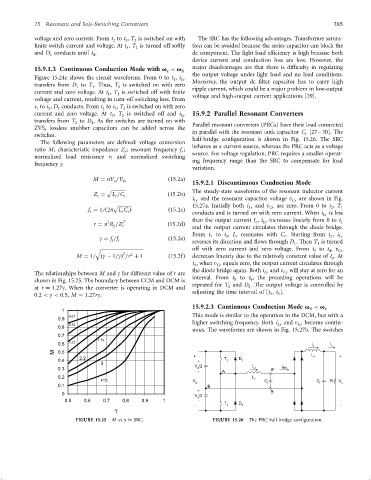
                   The following parameters are de®ned: voltage conversion
                                                                      behaves as a current source, whereas the PRC acts as a voltage
                 ratio M, characteristic impedance Z ; resonant frequency f ;
                                               r
                                                                  r
                 normalized load resistance r; and normalized switching  source. For voltage regulation, PRC requires a smaller operat-
                 frequency g.                                         ing frequency range than the SRC to compensate for load
                                                                      variation.
                                     M ¼ nV =V in             ð15:2aÞ  15.9.2.1 Discontinuous Conduction Mode
                                            o
                                          p               The steady-state waveforms of the resonant inductor current
                                     Z ¼   L =C r             ð15:2bÞ
                                      r
                                            r
                                                                      i Lr  and the resonant capacitor voltage v Cr  are shown in Fig.
                                            p              15.27a. Initially both i Lr  and v Cr  are zero. From 0 to t , T 1
                                                                                                                    2
                                   f ¼ 1=ð2p L C Þ            ð15:2cÞ  conducts and is turned on with zero current. When i Lr  is less
                                                r
                                    r
                                              r
                                                                      than the output current I , i Lr  increases linearly from 0 to t 1
                                                                                           o
                                          2
                                               T
                                     r ¼ n R =Z               ð15:2dÞ
                                            L  r                      and the output current circulates through the diode bridge.
                                                                      From t to t , L resonates with C . Starting from t , i Lr
                                                                                                     r
                                                                                                                    2
                                                                            1
                                                                                 3
                                                                                     r
                                       g ¼ f =f               ð15:2eÞ
                                           s  r                       reverses its direction and ¯ows through D . Then T is turned
                                                                                                                1
                                                                                                        1
                                                                      off with zero current and zero voltage. From t to t , v
                                      q                                      3    4  Cr
                                               2  2
                               M ¼ 1= ðg ÿ 1=gÞ =r þ 1        ð15:2fÞ  decreases linearly due to the relatively constant value of I .At
                                                                                                                     o
                                                                      t , when v  equals zero, the output current circulates through
                                                                       4      Cr
                                                                      the diode bridge again. Both i and v  will stay at zero for an
                 The relationships between M and g for different value of r are               Lr    Cr
                                                                      interval. From t to t , the preceding operations will be
                 shown in Fig. 15.25. The boundary between CCM and DCM is           5    9
                                                                      repeated for T and D . The output voltage is controlled by
                 at r ¼ 1:27g. When the converter is operating in DCM and         2      2
                                                                      adjusting the time interval of [t , t ].
                 0:2 < g < 0:5, M ¼ 1:27rg.                                                     4  5
                                                                      15.9.2.3 Continuous Conduction Mode v < v
                           1                                                                                 S    r
                                                                      This mode is similar to the operation in the DCM, but with a
                             0.67
                         0.9
                                                                      higher switching frequency. Both i  and v  become contin-
                             0.75                                                                 Lr     Cr
                         0.8
                                1                                     uous. The waveforms are shown in Fig. 15.27b. The switches
                         0.7
                                       1.73
                         0.6  1.27                                                                            i     I
                                                                                                              o     o
                        M  0.5                                                                                L
                                2.2                                   +          T    D                        f       +
                         0.4                                            +         1   1
                                        3                              V /2               I         i
                         0.3                                            d                 Lr    B'  B'B
                                                                        -       A
                         0.2                                                              L
                                        r=5                           V                    r  C                C    R  V
                         0.1                                           d   B                   r                f       o
                                                                        +                       B
                           0
                                                                       V /2
                                                                        d
                            0.5   0.6   0.7    0.8   0.9    1           -        T    D
                                                                       -          2   2                                -
                                            g
                               FIGURE 15.25  M vs g in SRC.                  FIGURE 15.26  The PRC half-bridge con®guration.
   290   291   292   293   294   295   296   297   298   299   300