
Page 297 - Rashid, Power Electronics Handbook
P. 297
15 Resonant and Soft-Switching Converters 287
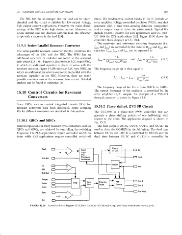
The PRC has the advantages that the load can be short- times. The fundamental control blocks in the IC include an
circuited and the circuit is suitable for low-output voltage, error ampli®er, voltage-controlled-oscillator (VCO), one-shot
high-output current applications. However, the major disad- generator with a zero wave-crossing detection comparator,
vantage of the PRC is the high device current. Moreover, as and an output stage to drive the active switch. Typical ICs
device current does not decrease with the load, the ef®ciency include UC1861-UC1864 for ZVS applications and UC 1865-
drops with a decrease in the load [29]. UC 1868 for ZCS applications [32]. Figure 15.30 shows the
controller block diagram of UC 1864.
The maximum and minimum switching frequencies (i.e.,
15.9.3 Series-Parallel Resonant Converter
f max and f min ) are controlled by the resistors R ange and R min and
The series-parallel resonant converter (SPRC) combines the capacitor C vco ; f max and f min can be expressed as
advantages of the SRC and the PRC. The SPRC has an
additional capacitor or inductor connected in the resonant 3:6 3:6
f max ¼ and f min ¼ ð15:3Þ
tank circuit [29 – 31]. Figure 15.29a shows an LCC-type SPRC, ðR ange =R min ÞC VCO R min C VCO
in which an additional capacitor is placed in series with the
resonant inductor. Figure 15.29b shows an LLC-type SPRC, in The frequency range Df is then equal to
which an additional inductor is connected in parallel with the
resonant capacitor in the SRC. However, there are many 3:6
Df ¼ f max ÿ f min ¼ ð15:4Þ
possible combinations of the resonant tank circuit. Detailed R ange C VCO
analysis can be found in Reference [31].
The frequency range of the ICs is from 10 kHz to 1 MHz.
The output frequency of the oscillator is controlled by the
15.10 Control Circuits for Resonant
error ampli®er (E=A) output. An example of a ZVS-MR
Converters forward converter is shown in Figure 15.31.
Since 1985s, various control integrated circuits (ICs) for 15.10.2 Phase-Shifted, ZVT FB Circuit
resonant converters have been developed. Some common
ICs for different converters are described in this section. The UCC3895 is a phase-shift PWM controller that can
generate a phase shifting pattern of one half-bridge with
respect to the other. The application diagram is shown in
15.10.1 QRCs and MRCs
Fig. 15.32.
Output regulations in many resonant-type converters, such as The four outputs OUTA, OUTB, OUTC, and OUTD are
QRCs and MRCs, are achieved by controlling the switching used to drive the MOSFETs in the full-bridge. The dead time
frequency. The ZCS applications require controlled switch-on between OUTA and OUTB is controlled by DELAB and the
times while ZVS applications require controlled switch-off dead time between OUTC and OUTD is controlled by
FIGURE 15.30 Controller block diagram of UC1864 (Courtesy of Unitrode Corp. and Texas Instruments, www.ti.com).