
Page 294 - Rashid, Power Electronics Handbook
P. 294
284 S. Hui and H. Chung
15.9 Load Resonant Converters 1 cycle
V d
v Cr
Load resonant converters (LRCs) have many distinct features
2V O
over conventional power converters. Due to the soft commu-
i Lr
tation of the switches, no turn-off loss or stress is present. t 3
0 w 0 t
These LRCs are especially well-suited for high-power applica-
tions because they allow high-frequency operation for equip-
ment size=weight reduction, without sacri®cing conversion -2V O
ef®ciency and imposing extra stress on the switches. Basically, None None
LRCs can be divided into three different con®gurations, T 1 D 1 T 2 D 2
180 o 180 o
namely series resonant converters, parallel resonant converters, t 0 t 1 t 2 t 4 t 5
and series-parallel resonant converters. (a)
1 cycle
15.9.1 Series Resonant Converters i Lr
v Cr
Series resonant converters (SRCs) have their load connected in
series with the resonant tank circuit, which is formed by L r
and C [15, 27 – 29]. The half-bridge con®guration is shown in 0 w 0 t
r
Fig. 15.23. When the resonant inductor current i Lr is positive,
it ¯ows through T if T is on; otherwise it ¯ows through
1
1
diode D . When i is negative, it ¯ows through T if T is on;
2
2
2
Lr
otherwise it ¯ows through diode D . In steady-state symme-
1
trical operation, both active switches are operated in a D 2 T 1 D 1 T 2 D 2
complementary manner. Depending on the ratio between t 0 t 1 t 2 t 3
the switching frequency o and the converter resonant (b)
S
frequency o , the converter has several possible operating
r 1 cycle
modes.
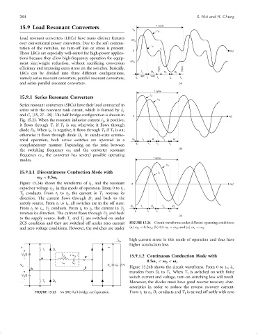
v Cr
15.9.1.1 Discontinuous Conduction Mode with i Lr
v < 0:5v r
S
Figure 15.24a shows the waveforms of i and the resonant
Lr 0 w 0 t
capacitor voltage v in this mode of operation. From 0 to t ,
Cr 1
T conducts. From t to t , the current in T reverses its
1 1 2 1
direction. The current ¯ows through D and back to the
1
supply source. From t to t , all switches are in the off state.
2 3
From t to t , T conducts. From t to t , the current in T D 1 T 1 D 2 T 2 D 1
3 4 2 4 5 2
t 0 t 1 t 2 t 3
reverses its direction. The current ¯ows through D and back
2 (c)
to the supply source. Both T and T are switched on under
1
2
ZCS condition and they are switched off under zero current FIGURE 15.24 Circuit waveforms under different operating conditions:
and zero voltage conditions. However, the switches are under (a) o S < 0:5o r ; (b) 0.5 o r < o S ; and (c) o r < o S .
I high current stress in this mode of operation and thus have
o
higher conduction loss.
+ T D +
+ 1 1
V /2 I +v -
d Lr Cr 15.9.1.2 Continuous Conduction Mode with
- A B'
r
S
L C 0:5v < v < v r
V r r V C R
d B o f Figure 15.24b shows the circuit waveforms. From 0 to t , i
B 1 Lr
+ transfers from D to T . When T is switched on with ®nite
2
1
1
V /2
d switch current and voltage, turn-on switching loss will result.
-
- T 2 D 2 - Moreover, the diodes must have good reverse recovery char-
acteristics in order to reduce the reverse recovery current.
FIGURE 15.23 An SRC half-bridge con®guration. From t to t , D conducts and T is turned off softly with zero
1
1
2
1