Page 293 - Rashid, Power Electronics Handbook
P. 293

15  Resonant and Soft-Switching Converters                                                          283

                                                                                  i     L
                                                                                   Lleak  leak         D1
                                                                                                  N:1
                                                          D                                                          +
                       S                                                                       +
                                                                              -
                                                                              V
                                                                               C  C            V                    V
                              D                  S                                  clamp       pri                  out
                                                                              +
                                                                           i
                                                                            Cclamp             -     i
                                                                                                     sec
                                                                                                                     -
                            (a) Buck                (b) Boost
                                                                                    S2
                                                                             V in            S1
                                                                                                          C
                                                                                                           DS
                               D
                       S
                                                 S       D
                                                                                               (a)
                          (c) Buck-boost             (d) Cuk
                                                                       S1
                                                                         0
                                                                       S2
                                  D                                      0
                                               S
                                                                       V +NV
                                                                        in  O
                                                                       V
                                                                        S1
                        S                                D               0
                                                                       i
                                                                        Lm
                                                                         0
                                                                         V
                            (e) Sepic                (f) Zeta             in
                                                                       V
                                                                        pri
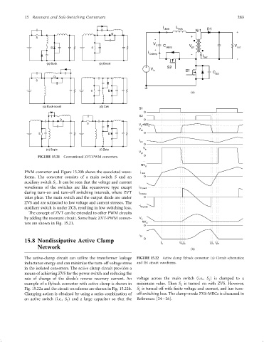
                        FIGURE 15.21  Conventional ZVT-PWM converters.   0
                                                                         -
                                                                        NV
                                                                          O
                 PWM converter and Figure 15.20b shows the associated wave-  i Lleak
                 forms. The converter consists of a main switch S and an  0
                 auxiliary switch S . It can be seen that the voltage and current
                                1
                 waveforms of the switches are like squarewave type except  i S1,peak
                 during turn-on and turn-off switching intervals, where ZVT  i Cclamp
                 takes place. The main switch and the output diode are under  0
                 ZVS and are subjected to low voltage and current stresses. The
                                                                       -i
                 auxiliary switch is under ZCS, resulting in low switching loss.  S1,peak
                   The concept of ZVT can be extended to other PWM circuits
                 by adding the resonant circuit. Some basic ZVT-PWM conver-  V C
                 ters are shown in Fig. 15.21.                          NV O
                                                                         0

                                                                       i
                                                                        D1  0
                 15.8 Nondissipative Active Clamp                                t        t  t t         t t  t t
                        Network                                                   0        1 2  3  (b)   4  5  6  7

                 The active-clamp circuit can utilize the transformer leakage  FIGURE 15.22  Active clamp ¯yback converter: (a) Circuit schematics;
                 inductance energy and can minimize the turn-off voltage stress  and (b) circuit waveforms.
                 in the isolated converters. The active clamp circuit provides a
                 means of achieving ZVS for the power switch and reducing the
                 rate of change of the diode's reverse recovery current. An  voltage across the main switch (i.e., S ) is clamped to a
                                                                                                        1
                 example of a ¯yback converter with active clamp is shown in  minimum value. Then S is turned on with ZVS. However,
                                                                                           2
                 Fig. 15.22a and the circuit waveforms are shown in Fig. 15.22b.  S is turned off with ®nite voltage and current, and has turn-
                                                                       2
                 Clamping action is obtained by using a series combination of  off switching loss. The clamp-mode ZVS-MRCs is discussed in
                 an active switch (i.e., S ) and a large capacitor so that the  References [24 – 26].
                                     2
   288   289   290   291   292   293   294   295   296   297   298