Page 72 - Rashid, Power Electronics Handbook
P. 72

4 Gate Turn-Off Thyristors                                                                           57

                 electric ®eld in the n-base region is grossly distorted due to the  regenerative action commences, but the device does not latch
                 presence of the charge carriers and may result in premature  on (remain on when the gate current is removed) until
                 avalanche breakdown. The resulting impact ionization can
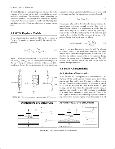
                 cause device failure. This phenomenon is known as ‘‘dynamic             a npn  þ a pnp    1        ð4:2Þ
                 avalanche.'' The device regains its steady-state blocking char-
                 acteristics when the tail current diminishes to leakage current
                                                                      This process takes only a short time for the current and the
                 level.
                                                                      current gains to increase enough to satisfy Eq. (4.2). For
                                                                      anode-shorted devices, the mechanism is similar but the
                                                                      anode short impairs the turn-on process by providing a
                 4.3 GTO Thyristor Models                             base–emitter short, thus reducing the p-n-p transistor gain,
                                                                      which is shown in Fig. 4.4. The composite p-n-p gain of the
                                                                      emitter-shorted structure is given as follows:
                 A one-dimensional two-transistor GTO model is shown in
                 Fig. 4.3. The device is expected to yield the turn-off gain g
                 given by:                                                       a   ðcompositeÞ¼ a  1 ÿ V be       ð4:3Þ
                                                                                  pnp
                                                                                                  pnp
                                                                                                      R Sanode
                                     I A     a npn                    where V ¼ emitter base voltage (generally 0.6 V for injection
                                A ¼    ¼                        ð4:1Þ        be
                                 g
                                     I G  a pnp  þ a npn  ÿ 1         of carriers) and R is the anode-short resistance. The anode
                                                                                     S
                                                                      emitter injects when the voltage around it exceeds 0.06 V, and
                                                                      therefore the collector current of the n-p-n transistor ¯owing
                 where I is the anode current and I the gate current at turn-  through the anode shorts in¯uences turn-on. The GTO
                                              G
                       A
                 off, and a npn  and a pnp  are the common-base current gains in  remains in a transistor state if the load circuit limits the
                 the n-p-n and p-n-p transistor sections of the device. For a  current through the shorts.
                 nonshorted device, the charge is drawn from the anode and
                                                                      4.4 Static Characteristics
                         Anode              A           A
                                                                      4.4.1 On-State Characteristics
                                                                      In the on-state, the GTO operates in a similar manner to the
                                                               apnp
                                                                      thyristor. If the anode current remains above the holding
                                                                      current level then positive gate drive may be reduced to zero
                  Gate           G                  G
                                                               anpn   and the GTO will remain in conduction. However, as a result
                                                                      of the turn-off ability of the GTO, it does possess a higher
                                                                      holding current level than the standard thyristor and, in
                                                             C        addition, the cathode of the GTO thyristor is subdivided
                        Cathode           C                           into small ®nger elements to assist turn-off. Thus, if the
                                                                      GTO thyristor anode current transiently dips below the hold-
                   FIGURE 4.3  Two-transistor model representing the GTO thyristor.  ing current level, localized regions of the device may turn off,


                                                 FIGURE 4.4  Two-transistor models of GTO structures.
   67   68   69   70   71   72   73   74   75   76   77