
Page 75 - Rashid, Power Electronics Handbook
P. 75
60 M. H. Rashid
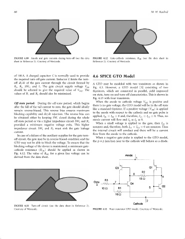
FIGURE 4.10 Anode and gate currents during turn-off (see the data FIGURE 4.12 Gate-cathode resistance, R GK (see the data sheet in
sheet in Reference 2). Courtesy of Westcode. Reference 2). Courtesy of Westcode.
of 100 A. A charged capacitor C is normally used to provide 4.6 SPICE GTO Model
the required turn-off gate current. Inductor L limits the turn-
off di=dt of the gate current through the circuit formed by A GTO may be modeled with two transistors as shown in
R ; R ; SW , and L. The gate circuit supply voltage V GS Fig. 4.3. However, a GTO model [3] consisting of two
2
1
1
should be selected to give the required value of V GQ . The thyristors, which are connected in parallel, yield improved
values of R and R should also be minimized.
1 2 on-state, turn-on and turn-off characteristics. This is shown in
Fig. 4.13 with four transistors.
When the anode to cathode voltage V AK is positive and
Off-state period: During the off-state period, which begins
there is no gate voltage, the GTO model will be in the off state
after the fall of the tail current to zero, the gate should ideally like a standard thyristor. If a positive voltage (V ) is applied
AK
remain reverse-biased. This reverse bias ensures maximum to the anode with respect to the cathode and no gate pulse is
blocking capability and dv=dt rejection. The reverse bias can
applied, I ¼ I ¼ 0 and, therefore, I ¼ I ¼ 0. Thus, no
C1
B2
B1
be obtained either by keeping SW closed during the whole anode current will ¯ow and I ¼ I ¼ 0. C2
1
off-state period or via a higher impedance circuit SW and R 3 A K
2
provided a minimum negative voltage exits. This higher When a small voltage is applied to the gate, then I B2 is
impedance circuit SW and R must sink the gate leakage nonzero and, therefore, both I C1 ¼ I C2 ¼ 0 are nonzero. Thus
3
2
current. the internal circuit will conduct and there will be a current
¯ow from the anode to the cathode.
In case of a failure of the auxiliary supplies for the gate turn-
When a negative gate pulse is applied to the GTO model,
off circuit, the gate may be in reverse-biased condition and the
the p-n-p junction near to the cathode will behave as a diode.
GTO may not be able to block the voltage. To ensure that the
blocking voltage of the device is maintained, a minimum gate-
cathode resistance (R ) should be applied as shown in
GK
Fig. 4.12. The value of R for a given line voltage can be
GK
derived from the data sheet.
FIGURE 4.11 Turn-off circuit (see the data sheet in Reference 2).
Courtesy of Westcode. FIGURE 4.13 Four-transistor GTO model. Courtesy of Westcode.