
Page 79 - Rashid, Power Electronics Handbook
P. 79
5 Power Bipolar Transistors 65
injected across the base-emitter junction, and holes injected Collector Emitter
from the base into the emitter. The emitter current is expo- Base Base
nentially related to the base-emitter voltage by the equation:
n Emitter Collector
i ¼ i e BE ÿ 1 ð5:1Þ
E E0 Z n T (a) (b)
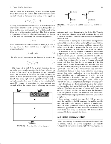
FIGURE 5.4 Circuit symbols (a) NPN transistor; and (b) PNP tran-
where i is the saturation current of the base-emitter junction sistor.
E
and which is a function of the doping levels, temperature and
the area of the base-emitter junction, V is the thermal voltage
T
Kt=q and Z is the emission coef®cient. The electron current resistance and power dissipation in the device [2]. There is
arriving at the collector junction can be expressed as a fraction an intermediate collector region with moderate doping, and
a of the total current crossing the base-emitter junction the emitter region is controlled so as to have a homogeneous
electrical ®eld.
i ¼ ai E ð5:2Þ Optimization of doping and base thickness are required to
C
achieve high breakdown voltage and ampli®cation capabilities.
Because the transistor is a three-terminals device, i is equal to Power transistors have their emitters and bases interleaved to
E
i þ i , hence the base current can be expressed as the reduce parasitic ohmic resistance in the base current path,
B
C
remaining fraction, which also improves the device for second breakdown failure.
The transistor is usually designed to maximize the emitter
i ¼ð1 ÿ aÞi ð5:3Þ
B E periphery per unit area of silicon, in order to achieve the
highest current gain at a speci®c current level. In order to
The collector and base currents are thus related by the ratio ensure those transistors have the greatest possible safety
margin, they are designed to be able to dissipate substantial
i c ¼ a ¼ b ð5:4Þ power and, thus, have low thermal resistance. It is for this
i 1 ÿ a
B reason, among others, that the chip area must be large and
that the emitter periphery per unit area is sometimes not
The values of a and b for a given transistor depend
optimized. Most transistor manufacturers use aluminum
primarily on the doping densities in the base, collector and
metallization because it has many attractive advantages,
emitter regions, as well as on the device geometry. Recombi-
among them easier application via vapor deposition and
nation and temperature also affect the values for both para- easier de®nition with photolithography. A major problem
meters. A power transistor requires a large blocking voltage in with aluminum is that only a thin layer can be applied by
the off state and a high current capability in the on state; a normal vapor-deposition techniques. Thus, when high
vertically oriented four-layer structure as shown in Fig. 5.3 is
currents are applied along the emitter ®ngers, a voltage drop
preferable because it maximizes the cross-sectional area
occurs along them, and the injection ef®ciency on the portions
through which the current ¯ows, enhancing the on-state
of the periphery that are farthest from the emitter contact is
reduced. This limits the amount of current each ®nger can
Base Emitter conduct. If copper metallization is substituted for aluminum,
then it is possible to lower the resistance from the emitter
N + contact to the operating regions of the transistors (the emitter
periphery).
P From a circuit point of view, Eqs. (5.1)–(5.4) are used to
relate the variables of the BJT input port (formed by base (B)
and emitter (E)) to the output port (collector (C) and emitter
(E)). The circuit symbols are shown in Fig. 5.4. Most of power
electronics applications use NPN transistors because electrons
+
N
move faster than holes, and therefore, NPN transistors have
considerable faster commutation times.
- 5.3 Static Characteristics
N
Collector Device static ratings determine the maximum allowable limits
of current, voltage, and power dissipation. The absolute
FIGURE 5.3 Power transistor vertical structure. voltage limit mechanism is concerned with the avalanche in