
Page 81 - Rashid, Power Electronics Handbook
P. 81
5 Power Bipolar Transistors 67
i limit Pulsed-SOA
C
i C quasi-saturation i C P limit
tot
i CM
breakdown
hard constant-current Secondary
breakdown
saturation limit
i b < 0 V limit
CE
(V CEO )
i b = 0 V CE V CE
BV CE0
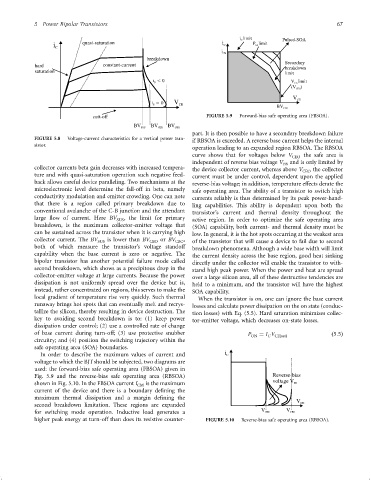
cutt-off FIGURE 5.9 Forward-bias safe operating area (FBSOA).
BV SUS BV CEO BV CBO
part. It is then possible to have a secondary breakdown failure
FIGURE 5.8 Voltage-current characteristics for a vertical power tran-
if RBSOA is exceeded. A reverse base current helps the internal
sistor.
operation leading to an expanded region RBSOA. The RBSOA
curve shows that for voltages below V CEO the safe area is
independent of reverse bias voltage V EB and is only limited by
collector currents beta gain decreases with increased tempera- the device collector current, whereas above V CEO the collector
ture and with quasi-saturation operation such negative feed- current must be under control, dependent upon the applied
back allows careful device paralleling. Two mechanisms at the reverse-bias voltage; in addition, temperature effects derate the
microelectronic level determine the fall-off in beta, namely safe operating area. The ability of a transistor to switch high
conductivity modulation and emitter crowding. One can note currents reliably is thus determined by its peak power-hand-
that there is a region called primary breakdown due to ling capabilities. This ability is dependent upon both the
conventional avalanche of the C-B junction and the attendant transistor's current and thermal density throughout the
large ¯ow of current. Here BV , the limit for primary
SUS active region. In order to optimize the safe operating area
breakdown, is the maximum collector-emitter voltage that (SOA) capability, both current- and thermal density must be
can be sustained across the transistor when it is carrying high low. In general, it is the hot spots occurring at the weakest area
collector current. The BV SUS is lower than BV CEO or BV CBO , of the transistor that will cause a device to fail due to second
both of which measure the transistor's voltage standoff breakdown phenomena. Although a wide base width will limit
capability when the base current is zero or negative. The the current density across the base region, good heat sinking
bipolar transistor has another potential failure mode called directly under the collector will enable the transistor to with-
second breakdown, which shows as a precipitous drop in the stand high peak power. When the power and heat are spread
collector-emitter voltage at large currents. Because the power over a large silicon area, all of these destructive tendencies are
dissipation is not uniformly spread over the device but is, held to a minimum, and the transistor will have the highest
instead, rather concentrated on regions, this serves to make the SOA capability.
local gradient of temperature rise very quickly. Such thermal When the transistor is on, one can ignore the base current
runaway brings hot spots that can eventually melt and recrys- losses and calculate power dissipation on the on state (conduc-
tallize the silicon, thereby resulting in device destruction. The tion losses) with Eq. (5.5). Hard saturation minimizes collec-
key to avoiding second breakdown is to: (1) keep power tor-emitter voltage, which decreases on-state losses.
dissipation under control; (2) use a controlled rate of change
of base current during turn-off; (3) use protective snubber P ON ¼ I V CEðsatÞ ð5:5Þ
C
circuitry; and (4) position the switching trajectory within the
safe operating area (SOA) boundaries.
In order to describe the maximum values of current and i C
voltage to which the BJTshould be subjected, two diagrams are
used: the forward-bias safe operating area (FBSOA) given in
Fig. 5.9 and the reverse-bias safe operating area (RBSOA) Reverse-bias
shown in Fig. 5.10. In the FBSOA current I is the maximum voltage V EB
CM
current of the device and there is a boundary de®ning the
maximum thermal dissipation and a margin de®ning the
V CE
second breakdown limitation. These regions are expanded
for switching mode operation. Inductive load generates a V CE0 V CB0
higher peak energy at turn-off than does its resistive counter- FIGURE 5.10 Reverse-bias safe operating area (RBSOA).