Page 80 - Rashid, Power Electronics Handbook
P. 80

Simo
                                                                                                                    ˜e
                                                                                                       M.
                                                                                                          Godoy
               66                                                                                      M. Godoy Simo˜es s
               66
                         i B                      i C

                                               V CE, sat
                                                                                      Increasing
                                                                                      base current


                                    V  BE                                              V CE


                               V f         Saturation       Constant-current

                                           region           ( active) region
                                                            i= i b B
                                                             C
                                         ( a)                                                               ( b)

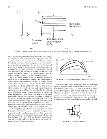
                      FIGURE 5.5  Family of current-voltage characteristic curves. (a) base-emitter input port; and (b) collector-emitter output port.


               terms of preventing thermal runaway. Forward current ratings
                                                                                       o
               are speci®ed at which the junction temperature does not      V = 2 V ( 125  C)
                                                                        )  b  CE
               exceed a rated value so as to prevent leads and contacts                              V = 400 V ( 25  C)
                                                                                                                o
               from being evaporated. Power dissipated in a semiconductor                             CE
               device produces a temperature rise and is related to thermal
               resistance. A family of voltage-current characteristic curves is  Current Gain (
                                                                                                o
               shown in Fig. 5.5. Figure 5.5a shows the base current i plotted        V = 2 V ( 25  C)
                                                                                       CE
                                                          B
               as a function of the base-emitter voltage v BE  and Fig. 5.5b
               depicts the collector current i as a function of the collector-
                                        C
               emitter voltage V , with i as the controlling variable.                                     log( )
                                                                                                              i
                              CE
                                     B
                 Figure 5.5 shows several curves distinguished from each                                       C
               other by the value of the base current. The active region is  FIGURE 5.6  Current gain depends on temperature V CE and I C .
               de®ned where ¯at, horizontal portions of voltage-current
               curves show ‘‘constant'' i C  current, because the collector  Vertical-structure power transistors have an additional
               current does not change signi®cantly with v CE  for a given i .  region of operation called quasi-saturation, indicated in the
                                                                B
               Those portions are used only for small signal transistors
                                                                    characteristics curve of Fig. 5.8. Such a feature is a conse-
               operating as linear ampli®ers. On the other hand, switching
                                                                    quence of the lightly doped collector drift region where the
               power electronics systems require transistors to operate in  collector base junction supports a low reverse bias. If the
               either the saturation region where v CE  is small or in the cutoff  transistor enters the hard-saturation region the on-state power
               region where the current is zero and the voltage is upheld by  dissipation is minimized; there is, however, a tradeoff Ð
               the device. A small base current drives the ¯ow of a much  in quasi-saturation the stored charges are smaller. At high
               larger current between collector and emitter; such gain (called
               beta Ð Eq. (5.4)) depends upon temperature, V  and I .
                                                         CE     C
               Figure 5.6 shows current gain increase with increased collector
               voltage; gain falls off at both high and low current levels.
                 High voltage BJTs typically have low current gain, and hence
                                                                                            T 1
               Darlington-connected devices, as indicated in Fig. 5.7 are
               commonly used. Considering gains b and b for each one
                                               1     2                                            T 2
               of these transistors, the Darlington connection will have an
               increased gain of b þ b þ b b and diode D1 speeds up the                 D 1
                               1   2   1 2
               turn-off process by allowing the base driver to remove the
               stored charge on the transistor bases.                         FIGURE 5.7  Darlington-connected BJTs.
   75   76   77   78   79   80   81   82   83   84   85