
Page 78 - Rashid, Power Electronics Handbook
P. 78
Simo
Godoy
M.
64
64 M. Godoy Simo˜es s
˜e
1 Mhz 1 Mhz
Power 100 kHz Power
MOSFET
Frequency 10 kHz IGBT BJT Frequency 10 kHz MCT
MOSFET
100 kHz
MCT IGBT BJT
1 kHz 1 kHz
GT O GT O
T hyristor T hyristor
1 kV 2 kV 3 kV 4 kV 5 kV 1 kA 2 kA 3 kA
Voltage Current
(a) (b)
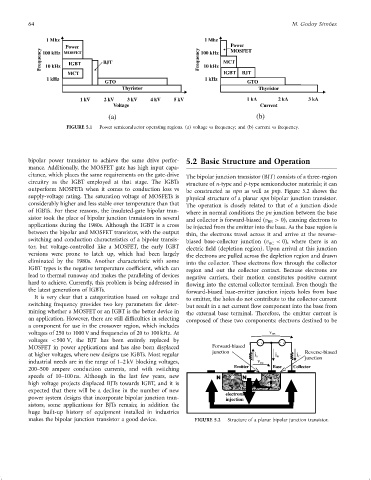
FIGURE 5.1 Power semiconductor operating regions. (a) voltage vs frequency; and (b) current vs frequency.
bipolar power transistor to achieve the same drive perfor- 5.2 Basic Structure and Operation
mance. Additionally, the MOSFET gate has high input capa-
citance, which places the same requirements on the gate-drive The bipolar junction transistor (BJT) consists of a three-region
circuitry as the IGBT employed at that stage. The IGBTs
structure of n-type and p-type semiconductor materials; it can
outperform MOSFETs when it comes to conduction loss vs
be constructed as npn as well as pnp. Figure 5.2 shows the
supply-voltage rating. The saturation voltage of MOSFETs is
physical structure of a planar npn bipolar junction transistor.
considerably higher and less stable over temperature than that
The operation is closely related to that of a junction diode
of IGBTs. For these reasons, the insulated-gate bipolar tran-
where in normal conditions the pn junction between the base
sistor took the place of bipolar junction transistors in several and collector is forward-biased ðv BE > 0Þ, causing electrons to
applications during the 1980s. Although the IGBT is a cross be injected from the emitter into the base. As the base region is
between the bipolar and MOSFET transistor, with the output thin, the electrons travel across it and arrive at the reverse-
switching and conduction characteristics of a bipolar transis- biased base-collector junction ðv BC < 0Þ, where there is an
tor, but voltage-controlled like a MOSFET, the early IGBT electric ®eld (depletion region). Upon arrival at this junction
versions were prone to latch up, which had been largely the electrons are pulled across the depletion region and drawn
eliminated by the 1980s. Another characteristic with some into the collector. These electrons ¯ow through the collector
IGBT types is the negative temperature coef®cient, which can region and out the collector contact. Because electrons are
lead to thermal runaway and makes the paralleling of devices negative carriers, their motion constitutes positive current
hard to achieve. Currently, this problem is being addressed in ¯owing into the external collector terminal. Even though the
the latest generations of IGBTs. forward-biased base-emitter junction injects holes from base
It is very clear that a categorization based on voltage and to emitter, the holes do not contribute to the collector current
switching frequency provides two key parameters for deter- but result in a net current ¯ow component into the base from
mining whether a MOSFET or an IGBT is the better device in the external base terminal. Therefore, the emitter current is
an application. However, there are still dif®culties in selecting composed of these two components: electrons destined to be
a component for use in the crossover region, which includes
voltages of 250 to 1000 V and frequencies of 20 to 100 kHz. At v CE
voltages <500 V, the BJT has been entirely replaced by _ + _ +
MOSFET in power applications and has also been displaced Forward-biased Reverse-biased
junction
at higher voltages, where new designs use IGBTs. Most regular i E i B i C junction
industrial needs are in the range of 1–2 kV blocking voltages, v BE
200–500 ampere conduction currents, and with switching Emitter Base Collector
speeds of 10–100 ns. Although in the last few years, new N P N holes
high voltage projects displaced BJTs towards IGBT, and it is flow
expected that there will be a decline in the number of new electrons
power system designs that incorporate bipolar junction tran- injection
sistors, some applications for BJTs remain; in addition the
huge built-up history of equipment installed in industries
makes the bipolar junction transistor a good device. FIGURE 5.2 Structure of a planar bipolar junction transistor.