Page 83 - Rashid, Power Electronics Handbook
P. 83

5 Power Bipolar Transistors                                                                          69

                         dI B     I B1                                                   +V cc
                         dt               2 I B  dI B
                                                  dt                                 R 1


                                                   I BR
                                                                                       T 1       C 1

                     FIGURE 5.14  Recommended base current for BJT driving.                                  T P
                                                                                                Z 1
                 slope and reverse current I BR  sweep out stored charges in the       T 2
                 transistor base, speeding up device turn-off.


                                                                         FIGURE 5.16  Base command without negative power supply.
                 5.5 Transistor Base Drive Applications
                                                                      and a positive current goes to T , thus keeping the capacitor
                 A plethora of circuits has been suggested to command tran-                      P
                                                                      charged with the Zener voltage; and when the input signal
                 sistors successfully for operation in power electronics switch-
                                                                      falls, T provides a path for the discharge of the capacitor,
                 ing systems [3]. Such base drive circuits try to satisfy the  2
                 following requirements: supply the right collector current;  which imposes a pulsed negative current from the base-emitter
                 adapt the base current to the collector current; and extract a  junction of T .
                                                                                 P
                                                                        A combination of large reverse base drive and antisaturation
                 reverse current from base to speed up device blocking. A good
                                                                      techniques may be used to reduce storage time to almost zero.
                 base driver reduces the commutation times and total losses,
                                                                      A circuit called Baker's clamp may be employed as illustrated
                 thus increasing ef®ciency and operating frequency. Depending
                                                                      in Fig. 5.17. When the transistor is on its base it is two diode
                 upon the grounding requirements between the control and the
                                                                      drops below the input. Assuming that diodes D and D have a
                 power circuits, the base drive might be either an isolated or                              2     3
                                                                      forward bias voltage of  0:7 V, then the base will be 1.4 V
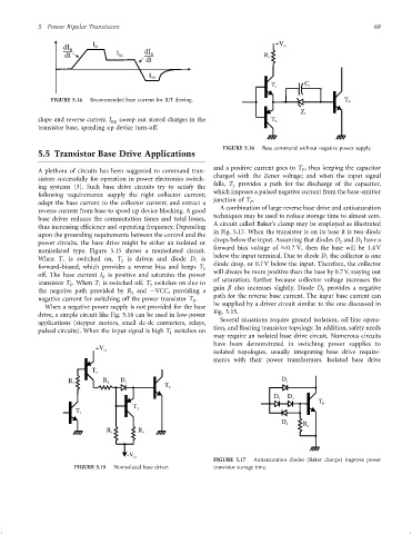
                 nonisolated type. Figure 5.15 shows a nonisolated circuit.
                                                                      below the input terminal. Due to diode D the collector is one
                 When T is switched on, T is driven and diode D is                                      1
                                                                1
                                          2
                         1
                 forward-biased, which provides a reverse bias and keeps T 3  diode drop, or 0.7 V below the input. Therefore, the collector
                 off. The base current I is positive and saturates the power  will always be more positive than the base by 0.7 V, staying out
                                     B
                 transistor T . When T is switched off, T switches on due to  of saturation; further because collector voltage increases the
                                                   3
                                    1
                           P
                                                                                                       4
                 the negative path provided by R and ÿVCC, providing a  gain b also increases slightly. Diode D provides a negative
                                             3
                 negative current for switching off the power transistor T .  path for the reverse base current. The input base current can
                                                                P
                   When a negative power supply is not provided for the base  be supplied by a driver circuit similar to the one discussed in
                                                                      Fig. 5.15.
                 drive, a simple circuit like Fig. 5.16 can be used in low-power
                                                                        Several situations require ground isolation, off-line opera-
                 applications (stepper motors, small dc-dc converters, relays,
                                                                      tion, and ¯oating transistor topology. In addition, safety needs
                 pulsed circuits). When the input signal is high T switches on
                                                         1
                                                                      may require an isolated base drive circuit. Numerous circuits
                                                                      have been demonstrated in switching power supplies to
                                   +V cc
                                                                      isolated topologies, usually integrating base drive require-
                                                                      ments with their power transformers. Isolated base drive
                                  T 2
                           R 1       R 2  D 1                                              D 1
                                                       T P
                                                                                        D 2  D 3
                                                                                                      T P
                                              T 3
                             T 1
                                                                                          D 4
                                                                                                 R 1
                                      R 3      R 4
                                            -V cc
                                                                      FIGURE 5.17  Antisaturation diodes (Baker clamps) improve power
                            FIGURE 5.15  Nonisolated base driver.     transistor storage time.
   78   79   80   81   82   83   84   85   86   87   88