
Page 82 - Rashid, Power Electronics Handbook
P. 82
M.
˜e
Simo
Godoy
68
68 M. Godoy Simo˜es s
5.4 Dynamic Switching Characteristics
Base voltage
Switching characteristics are important in de®ning device
velocity during change from conduction (on) to blocking
(off) states. Such transition velocity is of paramount impor-
tance because most of the losses are due to high frequency
switching. Figure 5.11 shows typical waveforms for a resistive
load. Index ‘‘r'' refers to the rising time (from 10 to 90% of Base current
maximum value); for example t is the current rise time and
ri
depends upon base current. The falling time is indexed by ‘‘f ''; t s t f
the parameter t is the current falling time, that is, when the
fi
transistor is blocking such time corresponds to crossing from
the saturation to the cutoff state. In order to improve t , the Collector current
fi
base current for blocking must be negative and the device t d t ri
must be kept in quasi-saturation so as to minimize stored t on t off
charges. The delay time is denoted by t , corresponding to the t fv t fv
d
time to discharge the capacitance of junction base-emitter,
which time can be reduced with a larger current base with high V CE, SAT
slope. Storage time (t ) is a very important parameter for BJT Voltage V CE
s
transistors, it is the time required to neutralize the carriers
stored in the collector and the base. Storage time and switch-
ing losses are key points when dealing with bipolar power Switching losses
transistors. Switching losses occur at both turn-on and turn-
off. For high-frequency operation the rising and falling times Power Conduction losses
for voltage and current transitions play an important role as
indicated by Fig. 5.12.
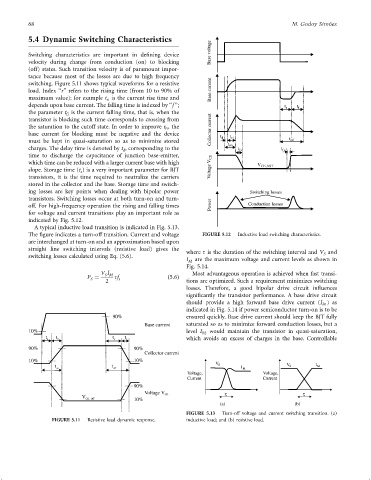
A typical inductive load transition is indicated in Fig. 5.13.
The ®gure indicates a turn-off transition. Current and voltage FIGURE 5.12 Inductive load switching characteristics.
are interchanged at turn-on and an approximation based upon
straight line switching intervals (resistive load) gives the
where t is the duration of the switching interval and V and
S
switching losses calculated using Eq. (5.6).
I M are the maximum voltage and current levels as shown in
Fig. 5.14.
V I Most advantageous operation is achieved when fast transi-
S M
P ¼ tf s ð5:6Þ
S
2 tions are optimized. Such a requirement minimizes switching
losses. Therefore, a good bipolar drive circuit in¯uences
signi®cantly the transistor performance. A base drive circuit
should provide a high forward base drive current (I )as
B1
indicated in Fig. 5.14 if power semiconductor turn-on is to be
90% ensured quickly. Base drive current should keep the BJT fully
Base current saturated so as to minimize forward conduction losses, but a
10% level I B2 would maintain the transistor in quasi-saturation,
t d t ri t s t f which avoids an excess of charges in the base. Controllable
90% 90%
Collector current
10% 10%
V S V S I M
t on t off I M
Voltage, Voltage,
Current Current
90%
Voltage V CE t t
10%
V CE, SAT
(a) (b)
FIGURE 5.13 Turn-off voltage and current switching transition. (a)
FIGURE 5.11 Resistive load dynamic response. inductive load; and (b) resistive load.