
Page 73 - Rashid, Power Electronics Handbook
P. 73
58 M. H. Rashid
thus forcing a high anode current back into the GTO at a high
rate of rise of anode current after this partial turn-off. This
situation could be potentially destructive. Therefore, it is
recommended that the positive gate drive not be removed
during conduction but held at a value I GðONÞ where I GðONÞ is
greater than the maximum critical trigger current (I )over
GT
the expected operating temperature range of the GTO thyr-
istor.
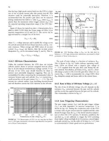
Figure 4.5 shows the typical on-state v-I characteristics for a
4000-A, 4500-V GTO from the Dynex range of GTOs [1] at
junction temperatures of 25 and 125 C. The curves can be
approximated to a straight line of the form:
V TM ¼ V þ IR 0 ð4:4Þ
0
where V ¼ voltage intercept and it models the voltage across
0
the cathode and anode forward-biased junctions, and R ¼on-
0
state resistance. When average and RMS values of on-state
current (I ; I ) are known, then the on-state power
TAV TRMS
dissipation P can be determined using V and R . That is,
ON 0 0 FIGURE 4.6 GTO blocking voltage vs R GK (see the data sheet in
Reference 1). GTO gate characteristic information reproduced by kind
2
P ON ¼ V I þ R I ð4:5Þ permission of Dynex Semiconductor.
0 TAV
0 TRMS
14.4.2 Off-State Characteristics The peak off-state voltage is a function of resistance R .
GK
This is shown in Fig. 4.6. Under ordinary operating condi-
Unlike the standard thyristor, the GTO does not include
tions, GTOs are biased with a negative gate voltage of
cathode emitter shorts to prevent nongated turn-on effects
ÿ15 V supplied from the gate drive unit during the off-
due to dv=dt-induced forward-biased leakage current. In the state interval. Nevertheless, provision of R may be a desir-
GK
off-state of the GTO, steps should therefore be taken to able design practice in the event the gate-drive failure for any
prevent such potentially dangerous triggering. This can be reason (R < 1:5O is recommended for a large GTO). Here
GK
accomplished by either connecting the recommended value of R dissipates energy and hence adds to the system losses.
resistance between gate and cathode (R GK ) or maintaining a GK
small reverse bias on the gate contact (V ¼ÿ2 V). This will
RG
prevent the cathode emitter from becoming forward-biased
and will therefore sustain the GTO thyristor in the off state. 4.4.3 Rate of Rise of Off-State Voltage (dv =dt)
T
The rate of rise of off-state voltage (dv =dt) depends on the
4000 Measured under pulse D
(A) conditions. resistance R GK connected between the gate and the cathode
I - I GIONI = 10A and the reverse bias applied between the gate and the cathode.
L 3000 Half sine wave 10 ms T = 25ºC This relationship is shown in Fig. 4.7.
I
current
on-state 2000 T = 125ºC 1.4.4 Gate Triggering Characteristics
I
The gate trigger current (I ) and the gate trigger voltage
GT
Instantaneous 1000 (V ) are both dependent on junction temperature T as
j
GT
shown in Fig. 4.8. During the conduction state of the GTO
a certain value of gate current must be supplied and this value
0
ture at which the GTO operates. In dynamic conditions the
1.0 1.5 2.0 2.5 3.0 3.5 4.0 should be larger than the I GT at the lowest junction tempera-
Instantaneous on-state voltage V -(V)
TM speci®ed I GT is not suf®cient to trigger the GTO switching
FIGURE 4.5 V-I Characteristics of GTO (see the data sheet in Refer- from higher voltage and high di=dt. In practice, a much higher
ence 1). GTO gate characteristic information reproduced by kind permis- peak gate current I GM (on the order of 10 times I )at T min
GT
j
sion of Dynex Semiconductor. is recommended to obtain good turn-on performance.