
Page 93 - Schaum's Outline of Theory and Problems of Electric Circuits
P. 93
AMPLIFIERS AND OPERATIONAL AMPLIFIER CIRCUITS
82
5.14 COMPARATOR [CHAP. 5
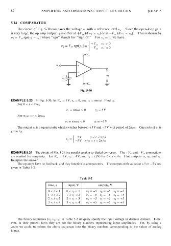
The circuit of Fig. 5-30 compares the voltage v 1 with a reference level v o . Since the open-loop gain
is very large, the op amp output v 2 is either at þV cc (if v 1 > v o )orat V cc (if v 1 < v o ). This is shown by
v 2 ¼ V cc sgn½v 1 v o where ‘‘sgn’’ stands for ‘‘sign of.’’ For v o ¼ 0, we have
v 1 > 0
þV cc
v 2 ¼ V cc sgn½v 1 ¼
V cc v 1 < 0
Fig. 5-30
EXAMPLE 5.23 In Fig. 5-30, let V cc ¼ 5V, v o ¼ 0, and v 1 ¼ sin !t. Find v 2 .
For 0 < t < =!,
v 1 ¼ sin !t > 0 v 2 ¼ 5V
For =! < t < 2 =!,
v 1 ¼ sin !t < 0 v 2 ¼ 5V
The output v 2 is a square pulse which switches between þ5 V and 5 V with period of 2 =!. One cycle of v 2 is
given by
5V 0 < t < =!
v 2 ¼
5V =! < t < 2 =!
EXAMPLE 5.24 The circuit of Fig. 5-31 is a parallel analog-to-digital converter. The þV cc and V cc connections
are omitted for simplicity. Let V cc ¼ 5V, v o ¼ 4 V, and v i ¼ t (V) for 0 < t < 4 s. Find outputs v 3 ; v 2 ; and v 1 .
Interpret the answer.
The op amps have no feedback, and they function as comparators. The outputs with values at þ5or 5 V are
given in Table 5-2.
Table 5-2
time, s input, V outputs, V
0 < t < 1 0 < v i < 1 v 3 ¼ 5 v 2 ¼ 5 v 1 ¼ 5
1 < t < 2 1 < v i < 2 v 3 ¼ 5 v 2 ¼ 5 v 1 ¼þ5
2 < t < 3 2 < v i < 3 v 3 ¼ 5 v 2 ¼þ5 v 1 ¼þ5
3 < t < 4 3 < v i < 4 v 3 ¼þ5 v 2 ¼þ5 v 1 ¼þ5
The binary sequences fv 3 ; v 2 ; v 1 g in Table 5-2 uniquely specify the input voltage in discrete domain. How-
ever, in their present form they are not the binary numbers representing input amplitudes. Yet, by using a
coder we could transform the above sequences into the binary numbers corresponding to the values of analog
inputs.