
Page 180 - Science at the nanoscale
P. 180
10:16
RPS: PSP0007 - Science-at-Nanoscale
June 5, 2009
Nanotools and Nanofabrication
170
of BE provides valuable information on the density and elements
distribution in the sample.
Sometimes the incident electron collides and removes an elec-
tron from the inner shell the sample atom, leaving a hole in the
orbital. An electron from a higher orbital will make a transi-
tion to this vacant lower energy level, filling the vacancy. Dur-
ing this transition, the difference in the energy is emitted in the
form of electromagnetic radiation. Typically this radiation falls
in the X-ray regime. The X-ray photons emitted in these pro-
cesses are unique to each element and can be used to identify
the elements in the sample. This technique requires an X-ray
detector, and is known as energy dispersive X-ray spectroscopy
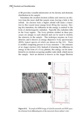
(EDX), typical spectra of which are shown in Fig. 8.11. There
is another competing process to X-ray emission — the emission
of an Auger electron (AE). Instead of releasing the difference in
energy in the form of a X-ray photon, this energy can be trans-
ferred to an electron occupying another outer shell, which leaves
the sample. Such an electron is known as the Auger Electron
Figure 8.11. Example of SEM image of hybrid nanorods and EDX spec- ch08
tra obtained fron different parts of the nanorods (from author’s lab).