
Page 178 - Science at the nanoscale
P. 178
10:16
RPS: PSP0007 - Science-at-Nanoscale
June 5, 2009
Nanotools and Nanofabrication
168
traveling through the SEM column. The objective lens focuses
The focal length
the electron beam onto the sample surface.
of the objective lens is denoted as the working distance of the
microscope.
The scanning of the electron beam over the surface of the sam-
ple is achieved by deflecting the beam using an applied electric
field or magnetic field. Typically a deflection coil consists of four
radially oriented coils arranged so that the magnetic field is per-
pendicular to the axis of the system. The magnetic field generated
by these coils can be controlled by the amount of electric cur-
rent passing through these coils. By programming these scanning
coils, one can readily raster the electron beam over the sample sur-
face.
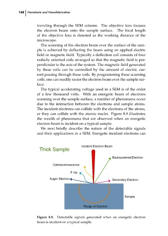
The typical accelerating voltage used in a SEM is of the order
of a few thousand volts. With an energetic beam of electrons
scanning over the sample surface, a number of phenomena occur
due to the interaction between the electrons and sample atoms.
The incident electrons can collide with the electrons of the atoms,
or they can collide with the atomic nuclei. Figure 8.9 illustrates
the wealth of phenomena that are observed when an energetic
electron beam is incident on a typical sample.
We next briefly describe the nature of the detectable signals
and their applications in a SEM. Energetic incident electrons can
Thick Sample
Catholuminescence Incident Electron Beam Backscattered Electron ch08
X-ray
Auger Electron Secondary Electron
Sample
Range of Electron
Figure 8.9. Detectable signals generated when an energetic electron
beam is incident on a typical sample.