
Page 182 - Science at the nanoscale
P. 182
10:16
RPS: PSP0007 - Science-at-Nanoscale
June 5, 2009
Nanotools and Nanofabrication
172
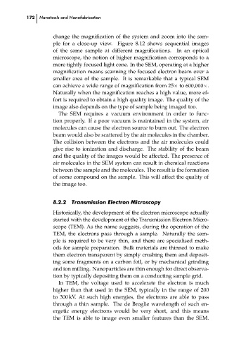
change the magnification of the system and zoom into the sam-
ple for a close-up view. Figure 8.12 shows sequential images
In an optical
of the same sample at different magnifications.
microscope, the notion of higher magnification corresponds to a
more tightly focused light cone. In the SEM, operating at a higher
magnification means scanning the focused electron beam over a
smaller area of the sample. It is remarkable that a typical SEM
can achieve a wide range of magnification from 25× to 600,000×.
Naturally when the magnification reaches a high value, more ef-
fort is required to obtain a high quality image. The quality of the
image also depends on the type of sample being imaged too.
The SEM requires a vacuum environment in order to func-
tion properly. If a poor vacuum is maintained in the system, air
molecules can cause the electron source to burn out. The electron
beam would also be scattered by the air molecules in the chamber.
The collision between the electrons and the air molecules could
give rise to ionization and discharge. The stability of the beam
and the quality of the images would be affected. The presence of
air molecules in the SEM system can result in chemical reactions
between the sample and the molecules. The result is the formation
of some compound on the sample. This will affect the quality of
the image too.
Transmission Electron Microscopy
8.2.2
Historically, the development of the electron microscope actually
started with the development of the Transmission Electron Micro-
scope (TEM). As the name suggests, during the operation of the
TEM, the electrons pass through a sample. Naturally the sam-
ple is required to be very thin, and there are specialised meth- ch08
ods for sample preparation. Bulk materials are thinned to make
them electron transparent by simply crushing them and deposit-
ing some fragments on a carbon foil, or by mechanical grinding
and ion milling. Nanoparticles are thin enough for direct observa-
tion by typically depositing them on a conducting sample grid.
In TEM, the voltage used to accelerate the electron is much
higher than that used in the SEM, typically in the range of 200
to 300kV. At such high energies, the electrons are able to pass
through a thin sample. The de Broglie wavelength of such en-
ergetic energy electrons would be very short, and this means
the TEM is able to image even smaller features than the SEM.