
Page 186 - Science at the nanoscale
P. 186
10:16
RPS: PSP0007 - Science-at-Nanoscale
June 5, 2009
Nanotools and Nanofabrication
176
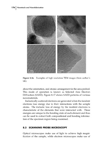
Examples of high resolution TEM images (from author’s
Figure 8.16.
lab).
about the orientation, and atomic arrangement in the area probed.
This mode of operation is known as Selected Area Electron
Diffraction (SAED). Figure 8.17 shows SAED patterns of various
nanomaterials.
Inelastically scattered electrons are generated when the incident ch08
electrons lose energy due to their interactions with the sample
atoms. The inelastic loss of energy by the incident electrons is
characteristic of the elements that were interacted with. These
energies are unique to the bonding state of each element and thus
can be used to extract both compositional and bonding informa-
tion of the specimen region being examined.
8.3 SCANNING PROBE MICROSCOPY
Optical microscopes make use of light to achieve high magni-
fication of the sample, while electron microscopes make use of