
Page 191 - Science at the nanoscale
P. 191
RPS: PSP0007 - Science-at-Nanoscale
10:16
June 5, 2009
8.3. Scanning Probe Microscopy
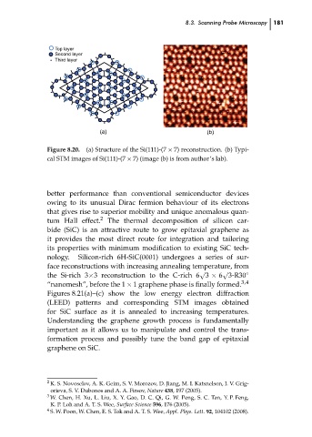
Top layer
Second layer
Third layer
(a)
(b)
Figure 8.20.
(a) Structure of the Si(111)-(7 × 7) reconstruction. (b) Typi-
cal STM images of Si(111)-(7 × 7) (image (b) is from author’s lab).
better performance than conventional semiconductor devices
owing to its unusual Dirac fermion behaviour of its electrons
that gives rise to superior mobility and unique anomalous quan-
2
The thermal decomposition of silicon car-
tum Hall effect.
bide (SiC) is an attractive route to grow epitaxial graphene as
it provides the most direct route for integration and tailoring
its properties with minimum modification to existing SiC tech-
Silicon-rich 6H-SiC(0001) undergoes a series of sur-
nology.
face reconstructions with increasing annealing temperature, from
√
√
the Si-rich 3×3 reconstruction to the C-rich 6 3 × 6 3-R30
◦
3,4
“nanomesh”, before the 1 × 1 graphene phase is finally formed.
Figures 8.21(a)–(c) show the low energy electron diffraction
(LEED) patterns and corresponding STM images obtained
for SiC surface as it is annealed to increasing temperatures. 181 ch08
Understanding the graphene growth process is fundamentally
important as it allows us to manipulate and control the trans-
formation process and possibly tune the band gap of epitaxial
graphene on SiC.
2 K. S. Novoselov, A. K. Geim, S. V. Morozov, D. Jiang, M. I. Katsnelson, I. V. Grig-
orieva, S. V. Dubonos and A. A. Firsov, Nature 438, 197 (2005).
3 W. Chen, H. Xu, L. Liu, X. Y. Gao, D. C. Qi, G. W. Peng, S. C. Tan, Y. P. Feng,
K. P. Loh and A. T. S. Wee, Surface Science 596, 176 (2005).
4 S. W. Poon, W. Chen, E. S. Tok and A. T. S. Wee, Appl. Phys. Lett. 92, 104102 (2008).