
Page 194 - Science at the nanoscale
P. 194
10:16
RPS: PSP0007 - Science-at-Nanoscale
June 5, 2009
Nanotools and Nanofabrication
184
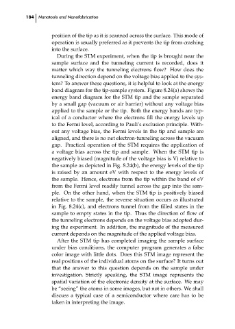
position of the tip as it is scanned across the surface. This mode of
operation is usually preferred as it prevents the tip from crashing
into the surface.
During the STM experiment, when the tip is brought near the
sample surface and the tunneling current is recorded, does it
matter which way the tunneling electrons flow? How does the
tunneling direction depend on the voltage bias applied to the sys-
tem? To answer these questions, it is helpful to look at the energy
band diagram for the tip-sample system. Figure 8.24(a) shows the
energy band diagram for the STM tip and the sample separated
by a small gap (vacuum or air barrier) without any voltage bias
applied to the sample or the tip. Both the energy bands are typ-
ical of a conductor where the electrons fill the energy levels up
to the Fermi level, according to Pauli’s exclusion principle. With-
out any voltage bias, the Fermi levels in the tip and sample are
aligned, and there is no net electron-tunneling across the vacuum
gap. Practical operation of the STM requires the application of
a voltage bias across the tip and sample. When the STM tip is
negatively biased (magnitude of the voltage bias is V) relative to
the sample as depicted in Fig. 8.24(b), the energy levels of the tip
is raised by an amount eV with respect to the energy levels of
the sample. Hence, electrons from the tip within the band of eV
from the Fermi level readily tunnel across the gap into the sam-
ple. On the other hand, when the STM tip is positively biased
relative to the sample, the reverse situation occurs as illustrated
in Fig. 8.24(c), and electrons tunnel from the filled states in the
sample to empty states in the tip. Thus the direction of flow of
the tunneling electrons depends on the voltage bias adopted dur-
ing the experiment. In addition, the magnitude of the measured
current depends on the magnitude of the applied voltage bias. ch08
After the STM tip has completed imaging the sample surface
under bias conditions, the computer program generates a false
color image with little dots. Does this STM image represent the
real positions of the individual atoms on the surface? It turns out
that the answer to this question depends on the sample under
investigation. Strictly speaking, the STM image represents the
spatial variation of the electronic density at the surface. We may
be “seeing” the atoms in some images, but not in others. We shall
discuss a typical case of a semiconductor where care has to be
taken in interpreting the image.