
Page 190 - Science at the nanoscale
P. 190
10:16
RPS: PSP0007 - Science-at-Nanoscale
June 5, 2009
Nanotools and Nanofabrication
180
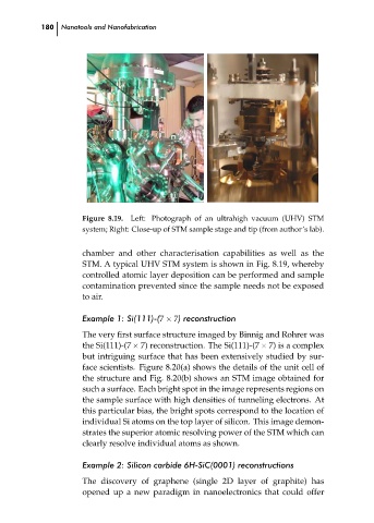
Left: Photograph of an ultrahigh vacuum (UHV) STM
Figure 8.19.
system; Right: Close-up of STM sample stage and tip (from author’s lab).
chamber and other characterisation capabilities as well as the
STM. A typical UHV STM system is shown in Fig. 8.19, whereby
controlled atomic layer deposition can be performed and sample
contamination prevented since the sample needs not be exposed
to air.
Example 1: Si(111)-(7 × 7) reconstruction
The very first surface structure imaged by Binnig and Rohrer was
the Si(111)-(7 × 7) reconstruction. The Si(111)-(7 × 7) is a complex
but intriguing surface that has been extensively studied by sur-
face scientists. Figure 8.20(a) shows the details of the unit cell of ch08
the structure and Fig. 8.20(b) shows an STM image obtained for
such a surface. Each bright spot in the image represents regions on
the sample surface with high densities of tunneling electrons. At
this particular bias, the bright spots correspond to the location of
individual Si atoms on the top layer of silicon. This image demon-
strates the superior atomic resolving power of the STM which can
clearly resolve individual atoms as shown.
Example 2: Silicon carbide 6H-SiC(0001) reconstructions
The discovery of graphene (single 2D layer of graphite) has
opened up a new paradigm in nanoelectronics that could offer