
Page 187 - Science at the nanoscale
P. 187
RPS: PSP0007 - Science-at-Nanoscale
10:16
June 5, 2009
8.3. Scanning Probe Microscopy
Figure 8.17.
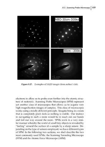
Examples of SAED images (from author’s lab).
electrons to allow us to probe even further into the atomic struc-
ture of materials. Scanning Probe Microscopes (SPM) represent
yet another class of microscopes that allows us to acquire very 177 ch08
high magnification images of samples. This class of microscopes
works using a totally different principle. Imagine being in a room
that is completely pitch dark so nothing is visible. Our instinct
in navigating in such a room would be to reach out our hands
and feel our way around the room. SPMs work in a very simi-
lar manner whereby the world of small tiny objects is revealed by
“feeling” around the surface of a sample by a sharp sensor. De-
pending on the type of sensors employed, we have different types
of SPM. In the following two sections, we shall describe the two
most commonly used SPMs: the Scanning Tunneling Microscope
(STM) and the Atomic Force Microscope (AFM).