
Page 192 - Science at the nanoscale
P. 192
10:16
RPS: PSP0007 - Science-at-Nanoscale
June 5, 2009
Nanotools and Nanofabrication
182
1100ºC
850ºC + Si flux
3X3
Graphene
(a)
(b)
(b)
(c)
(c)
(a)
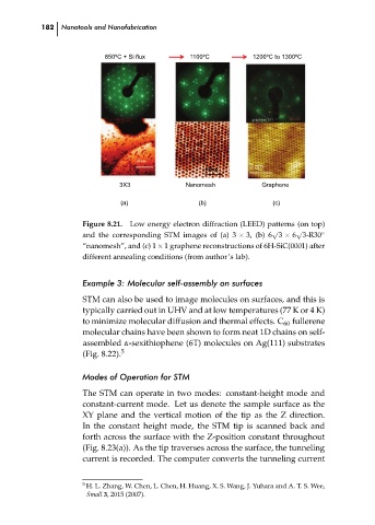
Figure 8.21.
Low energy electron diffraction (LEED) patterns (on top)
√
√
and the corresponding STM images of (a) 3 × 3, (b) 6 3 × 6 3-R30
“nanomesh”, and (c) 1 × 1 graphene reconstructions of 6H-SiC(0001) after
different annealing conditions (from author’s lab).
Example 3: Molecular self-assembly on surfaces
STM can also be used to image molecules on surfaces, and this is
typically carried out in UHV and at low temperatures (77 K or 4 K)
to minimize molecular diffusion and thermal effects. C 60 fullerene
molecular chains have been shown to form neat 1D chains on self-
assembled α-sexithiophene (6T) molecules on Ag(111) substrates
5
(Fig. 8.22).
Modes of Operation for STM Nanomesh 1200ºC to 1300ºC ◦ ch08
The STM can operate in two modes: constant-height mode and
constant-current mode. Let us denote the sample surface as the
XY plane and the vertical motion of the tip as the Z direction.
In the constant height mode, the STM tip is scanned back and
forth across the surface with the Z-position constant throughout
(Fig. 8.23(a)). As the tip traverses across the surface, the tunneling
current is recorded. The computer converts the tunneling current
5 H. L. Zhang, W. Chen, L. Chen, H. Huang, X. S. Wang, J. Yuhara and A. T. S. Wee,
Small 3, 2015 (2007).