
Page 196 - Science at the nanoscale
P. 196
10:16
RPS: PSP0007 - Science-at-Nanoscale
June 5, 2009
Nanotools and Nanofabrication
186
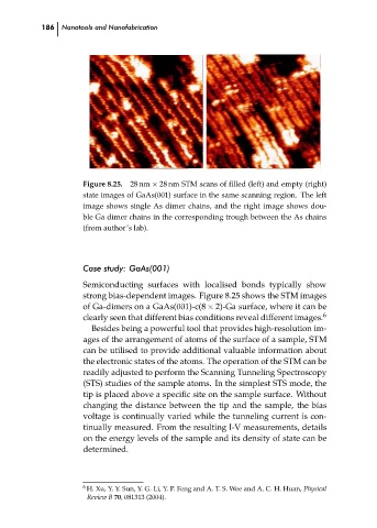
28 nm × 28 nm STM scans of filled (left) and empty (right)
Figure 8.25.
state images of GaAs(001) surface in the same scanning region. The left
image shows single As dimer chains, and the right image shows dou-
ble Ga dimer chains in the corresponding trough between the As chains
(from author’s lab).
Case study: GaAs(001)
Semiconducting surfaces with localised bonds typically show
strong bias-dependent images. Figure 8.25 shows the STM images
of Ga-dimers on a GaAs(001)-c(8 × 2)-Ga surface, where it can be
clearly seen that different bias conditions reveal different images.
Besides being a powerful tool that provides high-resolution im-
ages of the arrangement of atoms of the surface of a sample, STM
can be utilised to provide additional valuable information about
the electronic states of the atoms. The operation of the STM can be
readily adjusted to perform the Scanning Tunneling Spectroscopy 6 ch08
(STS) studies of the sample atoms. In the simplest STS mode, the
tip is placed above a specific site on the sample surface. Without
changing the distance between the tip and the sample, the bias
voltage is continually varied while the tunneling current is con-
tinually measured. From the resulting I-V measurements, details
on the energy levels of the sample and its density of state can be
determined.
6 H. Xu, Y. Y. Sun, Y. G. Li, Y. P. Feng and A. T. S. Wee and A. C. H. Huan, Physical
Review B 70, 081313 (2004).