Page 188 - Science at the nanoscale
P. 188

10:16
                                                     RPS: PSP0007 - Science-at-Nanoscale
                   June 5, 2009
                              Nanotools and Nanofabrication
                         178
                                                Feedback control for Piezotube
                                          Piezotube with
                                                     Current
                                                                              Control and
                                                     Amplifier
                                                                              Scanning Unit
                                            tip
                                           Tip
                                                                                 Display and
                                                                                 Data Processing
                                                                 Voltage
                                              Sample
                                                                     Ground
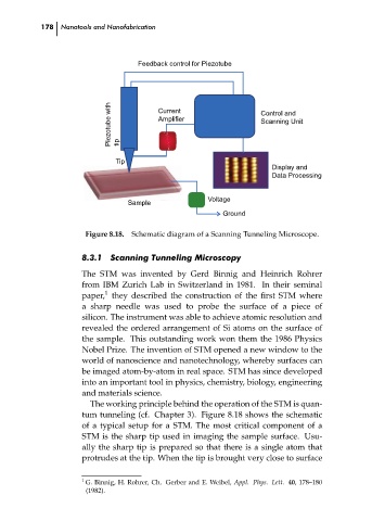
                                               Schematic diagram of a Scanning Tunneling Microscope.
                                    Figure 8.18.
                                          Scanning Tunneling Microscopy
                                   8.3.1
                                   The STM was invented by Gerd Binnig and Heinrich Rohrer
                                   from IBM Zurich Lab in Switzerland in 1981. In their seminal
                                         1
                                   paper, they described the construction of the first STM where
                                   a sharp needle was used to probe the surface of a piece of
                                   silicon. The instrument was able to achieve atomic resolution and
                                   revealed the ordered arrangement of Si atoms on the surface of
                                   the sample. This outstanding work won them the 1986 Physics
                                   Nobel Prize. The invention of STM opened a new window to the
                                   world of nanoscience and nanotechnology, whereby surfaces can
                                   be imaged atom-by-atom in real space. STM has since developed   ch08
                                   into an important tool in physics, chemistry, biology, engineering
                                   and materials science.
                                     The working principle behind the operation of the STM is quan-
                                   tum tunneling (cf. Chapter 3). Figure 8.18 shows the schematic
                                   of a typical setup for a STM. The most critical component of a
                                   STM is the sharp tip used in imaging the sample surface. Usu-
                                   ally the sharp tip is prepared so that there is a single atom that
                                   protrudes at the tip. When the tip is brought very close to surface
                                   1  G. Binnig, H. Rohrer, Ch. Gerber and E. Weibel, Appl. Phys. Lett. 40, 178–180
                                    (1982).
   183   184   185   186   187   188   189   190   191   192   193