
Page 184 - Science at the nanoscale
P. 184
10:16
RPS: PSP0007 - Science-at-Nanoscale
June 5, 2009
Nanotools and Nanofabrication
174
projection mode, the objective aperture is engaged and it enhances
contrast by blocking high-angle diffracted electrons. During the
diffraction pattern projection mode, the selected area aperture is
engaged and it facilitates the examination of the periodic diffrac-
tion of electrons caused by the interaction of the electrons with
the ordered arrangements of atoms in the sample. The formed
image then passes along the TEM column through the intermedi-
ate and projector lenses before it strikes the fluorescent screen. In
the image projection mode, the darker areas of the image repre-
sent those areas of the sample that fewer electrons are transmit-
ted through (thicker or denser); the lighter areas represent those
areas that more electrons are transmitted through (thinner or less
dense).
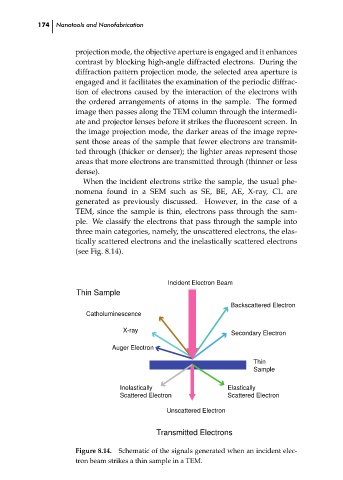
When the incident electrons strike the sample, the usual phe-
nomena found in a SEM such as SE, BE, AE, X-ray, CL are
generated as previously discussed. However, in the case of a
TEM, since the sample is thin, electrons pass through the sam-
ple. We classify the electrons that pass through the sample into
three main categories, namely, the unscattered electrons, the elas-
tically scattered electrons and the inelastically scattered electrons
(see Fig. 8.14).
Thin Sample
Catholuminescence
X-ray
Secondary Electron
Auger Electron Incident Electron Beam Backscattered Electron ch08
Thin
Sample
Inelastically Elastically
Scattered Electron Scattered Electron
Unscattered Electron
Transmitted Electrons
Figure 8.14. Schematic of the signals generated when an incident elec-
tron beam strikes a thin sample in a TEM.