
Page 179 - Science at the nanoscale
P. 179
RPS: PSP0007 - Science-at-Nanoscale
10:16
June 5, 2009
8.2. Electron Microscopy
collide with the electrons in the sample and knock them out of
their usual orbits. These electrons are known as Secondary Elec-
trons (SE). During the process, the incident electron loses little
energy and continues to generate more SE as it travels further
into the sample. A single incident electron will typically gener-
ate a shower of thousands of SE until the incident electron loses
its energy. Since a large number of SE are generated, the detec-
tion of SE is the most common mode of operation for SEM sample
imaging. Note that the SE have low energies so that SE generated
deep in the sample are unable to travel to the surface and leave
the sample. As a result, the SE detected are primarily from region
close to the sample surface (<10nm). Hence SE imaging would
produces good topographical information of the sample.
Sometimes an incident electron collides with the nucleus of a
sample atom, causing the electron to bounce back. Such electrons
are referred to as Backscattered Electrons (BE). Since the atomic
nucleus is more massive than the electron, the BE has high veloc-
ity and is characterized by its high energy (a few keV). High den-
sity samples will generally create more BE, and hence BE imaging
can be utilized to identify differences in the densities of a sam-
ple. The production of BE varies directly with the atomic num-
ber of the atoms in the sample. Therefore regions with atoms of
higher atomic number would appear brighter than regions with
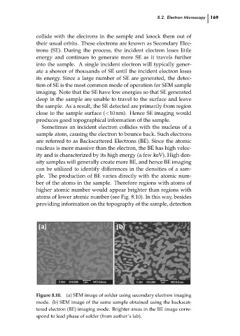
atoms of lower atomic number (see Fig. 8.10). In this way, besides
providing information on the topography of the sample, detection
Figure 8.10. (a) SEM image of solder using secondary electron imaging 169 ch08
mode. (b) SEM image of the same sample obtained using the backscat-
tered electron (BE) imaging mode. Brighter areas in the BE image corre-
spond to lead phase of solder (from author’s lab).