
Page 31 - Semiconductor For Micro- and Nanotechnology An Introduction For Engineers
P. 31
The Crystal Lattice System
(a) (b)
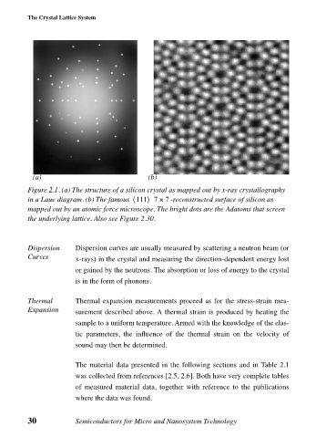
Figure 2.1. (a) The structure of a silicon crystal as mapped out by x-ray crystallography
〈
in a Laue diagram. (b) The famous 111〉 7 × 7 -reconstructed surface of silicon as
mapped out by an atomic force microscope. The bright dots are the Adatoms that screen
the underlying lattice. Also see Figure 2.30.
Dispersion Dispersion curves are usually measured by scattering a neutron beam (or
Curves x-rays) in the crystal and measuring the direction-dependent energy lost
or gained by the neutrons. The absorption or loss of energy to the crystal
is in the form of phonons.
Thermal Thermal expansion measurements proceed as for the stress-strain mea-
Expansion surement described above. A thermal strain is produced by heating the
sample to a uniform temperature. Armed with the knowledge of the elas-
tic parameters, the influence of the thermal strain on the velocity of
sound may then be determined.
The material data presented in the following sections and in Table 2.1
was collected from references [2.5, 2.6]. Both have very complete tables
of measured material data, together with reference to the publications
where the data was found.
30 Semiconductors for Micro and Nanosystem Technology