
Page 35 - Semiconductor For Micro- and Nanotechnology An Introduction For Engineers
P. 35
The Crystal Lattice System
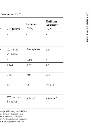
Gallium Arsenide GaAs - 5.65 - 0.31 350 ) (12 46 6 – 6.86×10
Process Si 3 N 4 - Amorphous 1902 0.26 750 18 6 – 2.7×10
Table 2.1. Lattice properties of the most important microsystem base materials a .
-Quartz 4.9127 5.4046 XY cut 14.3 Z cut 7.8
α 8.2 X i C - 0.169 740 1.4
Thermal Oxide SiO 2 18 14.4 – Amorphous 1705 - 0.22 0.17 740 - 1.5 1.1 6 – - 0.4×10 6 – 0.55×10
LPCVD Poly-Si 12.5 10.5 – , 5.43 polycrystal . 1412 0.3 0.2 – 702.24 150 6 – 2.33×10 a. The tabulated values for amorphous process materials are foundry-dependent and are provided only as an indica- tion of typical values. Also, many of the measurements on crystalline materials are for doped samples and henc
Crystalline Silicon Si : 100〉 ; 13 5.1 – : 11.7 111〉 5.43 1412 : 0.28 100〉 : 0.36 111〉 702.24 150 6 – 2.33×10
〈
〈
) 〈 〈
) ˜
Property Hardness (Gpa Lattice parameter () X, C: axes Melting point (°C Poisson ratio ν Specific heat kgK ⁄ J ( C p Thermal conductivity ) WmK ⁄ ( Thermal expansion coefficient 1 ) (T – α
32 Semiconductors for Micro and Nanosystem Technology