Page 37 - Semiconductor For Micro- and Nanotechnology An Introduction For Engineers
P. 37

The Crystal Lattice System
                                                      α T()
                                                                                   (2.1)
                                                      3
                                                     –
                                                                          4
                                                                          –
                              =  ( 3.725 1 –(  exp  – (  5.88×10 ( T –  124))) +  5.548×10 T)×10 – 6
                             and a lattice parameter (the interatomic distance in   ) that varies with
                             temperature as
                                                      aT()
                                                                                   (2.2)
                                                                      –
                                                 5
                                                –
                                                                                  2
                                                                      9
                             =  5.4304 +  1.8138×10 ( T –  298.15) +  1.542×10 ( T –  298.15)
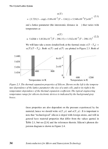
                             We will later take a more detailed look at the thermal strain ε T –(  T ) =
                                                                                   0
                                 (
                             α T() T –  T )  . Both α T()   and aT()   are plotted in Figure 2.3. Both of
                                       0
                    5.440                                – 6
                                                     4×10
                    5.438
                                                         – 6
                    5.436                            2×10
                                    400          800
                    5.434
                                                         0
                                                          0          600       1200
                               Temperature in K                 Temperature in K
                Figure 2.3. The thermal expansion properties of Silicon. Shown on the left is the tempera-
                ture dependence of the lattice parameter (the size of a unit cell), and to its right is the
                temperature dependence of the thermal expansion coefficient. The typical engineering
                temperature range for silicon electronic devices is indicated by the background gray
                boxes.


                             these properties are also dependent on the pressure experienced by the
                             material, hence we should write α Tp,(  )   and aT p,(  )  . It is important to
                             note that “technological” silicon is doped with foreign atoms, and will in
                             general have material properties that differ from the values quoted in
                             Table 2.1, but see [2.6] and the references therein. Silicon’s phonon dis-
                             persion diagram is shown in Figure 2.4.


                34           Semiconductors for Micro and Nanosystem Technology
   32   33   34   35   36   37   38   39   40   41   42