
Page 42 - Semiconductor For Micro- and Nanotechnology An Introduction For Engineers
P. 42
Crystal Structure
Gallium arsenide is mainly used to make devices and circuits for the all-
important opto-electronics industry, where its raw electronic speed or the
ability to act as an opto-electronic lasing device is exploited. It is not
nearly as popular as silicon, though, mainly because of the prohibitive
processing costs. Gallium arsenide has a number of material features that
differ significantly from Silicon, and hence a reason why we have
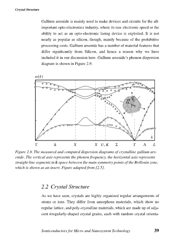
included it in our discussion here. Gallium arsenide’s phonon dispersion
diagram is shown in Figure 2.9.
ω k()
X
W U
K
Γ L
k
Γ ∆ X X UK, Σ Γ Λ L
Figure 2.9. The measured and computed dispersion diagrams of crystalline gallium ars-
enide. The vertical axis represents the phonon frequency, the horizontal axis represents
straight-line segments in k-space between the main symmetry points of the Brillouin zone,
which is shown as an insert. Figure adapted from [2.5].
2.2 Crystal Structure
As we have seen, crystals are highly organized regular arrangements of
atoms or ions. They differ from amorphous materials, which show no
regular lattice, and poly-crystalline materials, which are made up of adja-
cent irregularly-shaped crystal grains, each with random crystal orienta-
Semiconductors for Micro and Nanosystem Technology 39