
Page 38 - Semiconductor For Micro- and Nanotechnology An Introduction For Engineers
P. 38
Observed Lattice Property Data
ω k()
X
W U
K
Γ L
k k
Γ ∆ X UK, Σ Γ Λ LL K W X
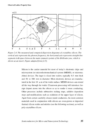
Figure 2.4. The measured and computed dispersion diagrams of crystalline silicon. The
vertical axis represents the phonon frequency, the horizontal axis represents straight-line
segments in k-space between the main symmetry points of the Brillouin zone, which is
shown as an insert. Figure adapted from [2.5].
Silicon is the carrier material for most of today’s electronic chips and
microsystem (or microelectromechanical system (MEMS), or microma-
chine) devices. The ingot is sliced into wafers, typically 0.5 mm thick
and 50 to 300 mm in diameter. Most electronic devices are manufac-
tured in the first 10 µ m of the wafer surface. MEMS devices can extend
all the way through the wafer. Cleanroom processing will introduce for-
eign dopant atoms into the silicon so as to render it more conducting.
Other processes include subtractive etching steps, additive deposition
steps and modifications such as oxidation of the upper layer of silicon.
Apart from certain carefully chosen metal conductors, the most common
materials used in conjunction with silicon are oven-grown or deposited
thermal silicon oxides and nitrides (see the following sections), as well as
poly-crystalline silicon.
Semiconductors for Micro and Nanosystem Technology 35