
Page 105 - Semiconductor Manufacturing Handbook
P. 105
Geng(SMH)_CH09.qxd 04/04/2005 19:42 Page 9.4
MICROLITHOGRAPHY
9.4 WAFER PROCESSING
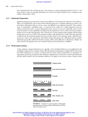
been transferred into the underlying layer. This sequence is shown diagrammatically in Fig. 9.1, and
most of these steps are generally performed on several tools linked together into a contiguous unit
called a lithographic cluster.
9.1.1 Substrate Preparation
Substrate preparation is intended to improve the adhesion of the photoresist material to the substrate.
This is accomplished by one or more of the following processes—substrate cleaning to remove con-
tamination, dehydration bake to remove water, and addition of an adhesion promoter. One common
type of contaminant—adsorbed water—is removed most readily by a high temperature process
called a dehydration bake. A typical dehydration bake, however, does not completely remove water
from the surface of silica substrates (including silicon, polysilicon, silicon oxide, and silicon nitride).
Surface silicon atoms bond strongly with a monolayer of water forming silanol groups (SiOH). Bake
temperatures in excess of 600°C are required to remove this final layer of water. Since this approach
is impractical, the preferred method of removing this silanol is by chemical means. Adhesion pro-
moters are used to react chemically with surface silanol and replace the -OH group with an organic
functional group that, unlike the hydroxyl group, offers good adhesion to photoresist. Silanes are
often used for this purpose, the most common being hexamethyldisilizane (HMDS).
9.1.2 Photoresist Coating
A thin, uniform coating of photoresist at a specific, well-controlled thickness is accomplished by the
seemingly simple process of spin coating. The photoresist, rendered into a liquid form by dissolving
the solid components in a solvent, is poured onto the wafer, which is then spun on a turntable at a
high speed, producing the desired film. Stringent requirements for thickness control and uniformity
and low-defect density call for particular attention to be paid to this process where a large number
Prepare wafer
Coat with photoresist
Prebake
Align and expose
Develop
Etch, implant, etc.
Strip resist
FIGURE 9.1 Example of a typical sequence of lithographic
processing steps (with no postexposure bake in this case), illus-
trated for a positive resist.
Downloaded from Digital Engineering Library @ McGraw-Hill (www.digitalengineeringlibrary.com)
Copyright © 2004 The McGraw-Hill Companies. All rights reserved.
Any use is subject to the Terms of Use as given at the website.