
Page 110 - Semiconductor Manufacturing Handbook
P. 110
Geng(SMH)_CH09.qxd 04/04/2005 19:42 Page 9.9
MICROLITHOGRAPHY
MICROLITHOGRAPHY 9.9
and gives more uniform developer coverage. Another in-line development strategy is called puddle
development. Again using developers specifically formulated for this process, the developer is
poured onto a stationary wafer that is then allowed to sit motionless for the duration of the develop-
ment time. The wafer is then spin rinsed and dried. Note that all three in-line processes can be per-
formed in the same piece of equipment with only minor modifications, and combinations of these
techniques are frequently used.
9.2 IMAGE FORMATION IN OPTICAL LITHOGRAPHY
Projection imaging tools are sophisticated reduction cameras with stages that allow, through a com-
bination of stepping or stepping and scanning motions, the exposure of many copies of a mask pat-
tern onto a large wafer. The image of the mask that is projected into the photoresist defines the
information content used by the photoresist to form the final resist image. Understanding the limits
and capabilities of projection imaging is the first step in understanding the limits and capabilities of
lithography.
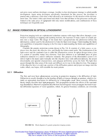
Consider the generic projection system shown in Fig. 9.6. It consists of a light source, a con-
denser lens, the mask, the objective lens, and finally the resist-coated wafer. The combination of the
light source and the condenser lens is called the illumination system. In optical design terms a lens
is a system of (possibly many) lens elements. Each lens element is an individual piece of glass
(refractive element) or a mirror (reflective element). The purpose of the illumination system is to
deliver light to the mask (and eventually into the objective lens) with sufficient intensity, the proper
directionality and spectral characteristics, and adequate uniformity across the field. The light then
passes through the clear areas of the mask and diffracts on its way to the objective lens. The purpose
of the objective lens is to pick up a portion of the diffraction pattern and project an image onto the
wafer, which, one hopes, will resemble the mask pattern.
9.2.1 Diffraction
The first and most basic phenomenon occurring in projection imaging is the diffraction of light.
Diffraction is usually thought of as the bending of light as it passes through an aperture, which is cer-
tainly an appropriate description for diffraction by a lithographic mask. More correctly, diffraction
theory simply describes how light propagates. This propagation includes the effects of the surround-
ings (boundaries). Maxwell’s equations describe how electromagnetic waves propagate, but result in par-
tial differential equations of vector quantities, which, for general boundary conditions, are extremely
Mask
Light source
Condenser lens
Objective lens
Wafer
FIGURE 9.6 Block diagram of a generic projection imaging system.
Downloaded from Digital Engineering Library @ McGraw-Hill (www.digitalengineeringlibrary.com)
Copyright © 2004 The McGraw-Hill Companies. All rights reserved.
Any use is subject to the Terms of Use as given at the website.