
Page 107 - Semiconductor Manufacturing Handbook
P. 107
Geng(SMH)_CH09.qxd 04/04/2005 19:42 Page 9.6
MICROLITHOGRAPHY
9.6 WAFER PROCESSING
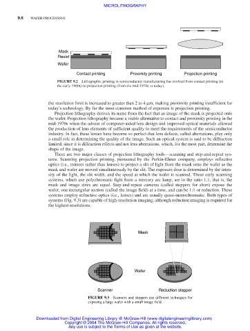
Mask
Resist
Wafer
Contact printing Proximity printing Projection printing
FIGURE 9.2 Lithographic printing in semiconductor manufacturing has evolved from contact printing (in
the early 1960s) to projection printing (from the mid-1970s to today).
the resolution limit is increased to greater than 2 to 4 µm, making proximity printing insufficient for
today’s technology. By far the most common method of exposure is projection printing.
Projection lithography derives its name from the fact that an image of the mask is projected onto
the wafer. Projection lithography became a viable alternative to contact and proximity printing in the
mid-1970s when the advent of computer-aided lens design and improved optical materials allowed
the production of lens elements of sufficient quality to meet the requirements of the semiconductor
industry. In fact, these lenses have become so perfect that lens defects, called aberrations, play only
a small role in determining the quality of the image. Such an optical system is said to be diffraction
limited, since it is diffraction effects and not lens aberrations, which, for the most part, determine the
shape of the image.
There are two major classes of projection lithography tools—scanning and step-and-repeat sys-
tems. Scanning projection printing, pioneered by the Perkin-Elmer company, employs reflective
optics (i.e., mirrors rather than lenses) to project a slit of light from the mask onto the wafer as the
mask and wafer are moved simultaneously by the slit. The exposure dose is determined by the inten-
sity of the light, the slit width, and the speed at which the wafer is scanned. These early scanning
systems, which use polychromatic light from a mercury arc lamp, are in the ratio 1:1, that is, the
mask and image sizes are equal. Step-and-repeat cameras (called steppers for short) expose the
wafer, one rectangular section (called the image field) at a time, and can be 1:1 or reduction. These
systems employ refractive optics (i.e., lenses) and are usually quasi-monochromatic. Both types of
systems (Fig. 9.3) are capable of high-resolution imaging, although reduction imaging is required for
the highest resolutions.
Mask
Wafer
Scanner Reduction stepper
FIGURE 9.3 Scanners and steppers use different techniques for
exposing a large wafer with a small image field.
Downloaded from Digital Engineering Library @ McGraw-Hill (www.digitalengineeringlibrary.com)
Copyright © 2004 The McGraw-Hill Companies. All rights reserved.
Any use is subject to the Terms of Use as given at the website.