
Page 108 - Semiconductor Manufacturing Handbook
P. 108
Geng(SMH)_CH09.qxd 04/04/2005 19:42 Page 9.7
MICROLITHOGRAPHY
MICROLITHOGRAPHY 9.7
Scanners replaced proximity printing by the mid-seventies for device geometries below 4 to 5 µm.
By the early 1980s, steppers began to dominate as device designs pushed to 2 µm and below. Steppers
have continued to dominate lithographic patterning throughout the 1990s as minimum feature sizes
reached the 250-nm levels. However, by the early 1990s, a hybrid step-and-scan approach was intro-
duced. The step-and-scan approach uses a fraction of a normal stepper field (e.g., 25 mm × 8 mm),
then scans this field in one direction to expose the entire 4 × reduction mask. The wafer is then stepped
to a new location and the scan is repeated. The smaller imaging field simplifies the design and man-
ufacture of the lens, but at the expense of a more complicated reticle and wafer stage. Step-and-scan
technology is the technology of choice today for below 250 nm manufacturing.
Resolution, the smallest feature that can be printed with adequate control, has two basic limits—
the smallest image that can be projected onto the wafer and the resolving capability of the photore-
sist to make use of that image. From the projection imaging side, resolution is determined by the
wavelength of the imaging light (l) and the numerical aperture (NA) of the projection lens, accord-
ing to the Rayleigh criterion
R ∝ l (9.1)
NA
Lithography systems have progressed from blue wavelengths (436 nm) to UV (365 nm) to deep
UV (248 nm) to today’s mainstream high-resolution wavelength of 193 nm. In the meantime, pro-
jection tool numerical apertures have risen from 0.16 for the first scanners, to amazingly high
0.93 NA systems today, producing features well under 100 nm in size.
Before the exposure of the photoresist with an image of the mask can begin, this image must be
aligned with the previously defined patterns on the wafer. This alignment, and the resulting overlay of
the two or more lithographic patterns, is critical since tighter overlay control means circuit features can
be packed closer together. Closer packing of devices through better alignment and overlay is nearly as
critical as smaller devices through higher resolution in the drive toward more functionality per chip.
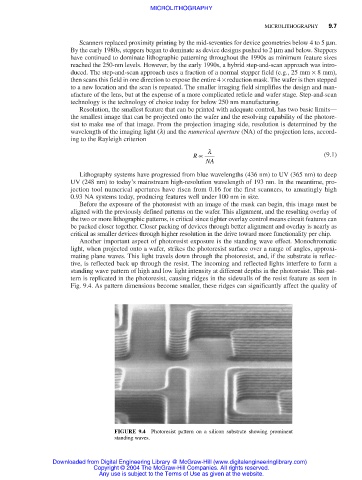
Another important aspect of photoresist exposure is the standing wave effect. Monochromatic
light, when projected onto a wafer, strikes the photoresist surface over a range of angles, approxi-
mating plane waves. This light travels down through the photoresist, and, if the substrate is reflec-
tive, is reflected back up through the resist. The incoming and reflected lights interfere to form a
standing wave pattern of high and low light intensity at different depths in the photoresist. This pat-
tern is replicated in the photoresist, causing ridges in the sidewalls of the resist feature as seen in
Fig. 9.4. As pattern dimensions become smaller, these ridges can significantly affect the quality of
FIGURE 9.4 Photoresist pattern on a silicon substrate showing prominent
standing waves.
Downloaded from Digital Engineering Library @ McGraw-Hill (www.digitalengineeringlibrary.com)
Copyright © 2004 The McGraw-Hill Companies. All rights reserved.
Any use is subject to the Terms of Use as given at the website.