
Page 109 - Semiconductor Manufacturing Handbook
P. 109
Geng(SMH)_CH09.qxd 04/04/2005 19:42 Page 9.8
MICROLITHOGRAPHY
9.8 WAFER PROCESSING
the feature. The interference that causes standing waves also results in a phenomenon called swing
curves, the sinusoidal variation in linewidth with changing resist thickness. These detrimental effects
are best cured by coating the substrate with a thin absorbing layer called a bottom antireflective coat-
ing (BARC) that can reduce the reflectivity seen by the photoresist to less than 1 percent.
9.1.5 Postexposure Bake
One method of reducing the standing wave effect is called the postexposure bake (PEB). Although
there is still some debate as to the mechanism, it is believed that the high temperatures used (100 to
130°C) cause diffusion of the exposed photosensitive material, thus smoothing out the standing wave
ridges. It has also been observed that the rate of diffusion is dependent on the prebake conditions
since the presence of solvent enhances diffusion during a PEB. Thus, a low temperature prebake
results in greater diffusion for a given PEB temperature. For a conventional resist, the main impor-
tance of the PEB is diffusion to remove standing waves. For another class of photoresists, called
chemically amplified resists, the PEB is an essential part of the chemical reactions that create a sol-
ubility differential between exposed and unexposed parts of the resist. For these resists, exposure
generates a small amount of a strong acid that does not itself change the solubility of the resist.
During the postexposure bake, this photogenerated acid catalyzes a reaction that changes the solu-
bility of the polymer resin in the resist. Since the photogenerated acid is not consumed in this reac-
tion, it continues to cause more solubility changing events and thus “amplifies” the effects of
exposure. Control of the PEB is extremely critical for chemically amplified resists.
9.1.6 Development
Once exposed, the photoresist must be developed. Most commonly used photoresists use aqueous bases
as developers. In particular, tetramethyl ammonium hydroxide (TMAH) is used almost universally at a
concentration of 0.26 N. Development is undoubtedly one of the most critical steps in the photoresist
process. The characteristics of the resist-developer interactions determine to a large extent the shape of
the photoresist profile and, more importantly, the control of the sizes of the features being printed.
The method of applying a developer to the photoresist is important in controlling the develop-
ment uniformity and process latitude. During spin development, wafers are spun using equipment
similar to that used for spin coating, and the developer is poured onto the rotating wafer. The wafer
is also rinsed and dried while still spinning. Spray development has been shown to have good results
using developers specifically formulated for this dispense method. Using a process identical to spin
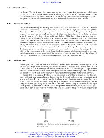
development, the developer is sprayed, rather than poured, on the wafer by using a nozzle that pro-
duces a fine mist of the developer over the wafer (Fig. 9.5). This technique reduces developer usage
Nozzle
Spray Puddle
FIGURE 9.5 Different developer application techniques are
commonly used.
Downloaded from Digital Engineering Library @ McGraw-Hill (www.digitalengineeringlibrary.com)
Copyright © 2004 The McGraw-Hill Companies. All rights reserved.
Any use is subject to the Terms of Use as given at the website.