
Page 115 - Semiconductor Manufacturing Handbook
P. 115
Geng(SMH)_CH09.qxd 04/04/2005 19:42 Page 9.14
MICROLITHOGRAPHY
9.14 WAFER PROCESSING
model for describing the phase error across the pupil is the Zernike polynomial, an infinite ortho-
normal polynomial series, usually cutoff at 36 terms, with powers of the radial pupil position and
trigonometric functions of the polar angle. The Zernike polynomial can be arranged in many ways,
but most lens design software and lens measuring equipment in use today employ a form called the
fringe or circle Zernike polynomial. Terms of this polynomial describe common aberrations such
as coma and astigmatism. The impact of these phase errors described by the Zernike polynomial
is to modify the pupil function of Eq. (9.5) to include this phase change on transmission through
the pupil.
Previous expressions for calculating the aerial image (such as Eqs. (9.2), (9.5), and (9.6)) apply
only to the image at the focal plane. What happens when the imaging system is out of focus? What
is the image intensity distribution some small distance away from the plane of best focus? The
impact of focus errors on the resulting aerial image can be described as an aberration of a sort.
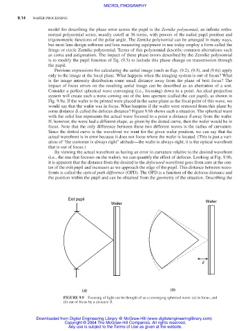
Consider a perfect spherical wave converging (i.e., focusing) down to a point. An ideal projection
system will create such a wave coming out of the lens aperture (called the exit pupil), as shown in
Fig. 9.9a. If the wafer to be printed were placed in the same plane as the focal point of this wave, we
would say that the wafer was in focus. What happens if the wafer were removed from this plane by
some distance d, called the defocus distance? Figure 9.9b shows such a situation. The spherical wave
with the solid line represents the actual wave focused to a point a distance d away from the wafer.
If, however, the wave had a different shape, as given by the dotted curve, then the wafer would be in
focus. Note that the only difference between these two different waves is the radius of curvature.
Since the dotted curve is the wavefront we want for the given wafer position, we can say that the
actual wavefront is in error because it does not focus where the wafer is located. (This is just a vari-
ation of “the customer is always right” attitude—the wafer is always right, it is the optical wavefront
that is out of focus.)
By viewing the actual wavefront as having an error in curvature relative to the desired wavefront
(i.e., the one that focuses on the wafer), we can quantify the effect of defocus. Looking at Fig. 9.9b,
it is apparent that the distance from the desired to the defocused wavefront goes from zero at the cen-
ter of the exit pupil and increases as we approach the edge of the pupil. This distance between wave-
fronts is called the optical path difference (OPD). The OPD is a function of the defocus distance and
the position within the pupil and can be obtained from the geometry of the situation. Describing the
Exit pupil Wafer
Wafer
d
(a) (b)
FIGURE 9.9 Focusing of light can be thought of as a converging spherical wave: (a) in focus, and
(b) out of focus by a distance d.
Downloaded from Digital Engineering Library @ McGraw-Hill (www.digitalengineeringlibrary.com)
Copyright © 2004 The McGraw-Hill Companies. All rights reserved.
Any use is subject to the Terms of Use as given at the website.