
Page 116 - Semiconductor Manufacturing Handbook
P. 116
Geng(SMH)_CH09.qxd 04/04/2005 19:42 Page 9.15
MICROLITHOGRAPHY
MICROLITHOGRAPHY 9.15
position within the exit pupil by an angle θ, the optical path difference is given by
OPD = δ (1 − cosθ) (9.7)
As we have seen before, the spatial frequency and the numerical aperture define positions with-
in the pupil as the sine of an angle. Thus, Eq. (9.7) will be more useful if expressed as a function of
sinq:
4
6
2
2
OPD = (1 − cos ) q = 1 d sin q + sin q + sin q + K ≈ 1 d sin q (9.8)
2 4 8 2
where the final approximation is accurate only for relatively small angles.
So how does this optical path difference affect the formation of an image? The OPD acts just
like an aberration, modifying the pupil function of the lens. For light, this path length traveled (the
OPD) is equivalent to a change in phase. Thus, the OPD can be expressed as a phase error ∆f due
to defocus:
=
−
)
/
/
(
∆f k OPD = 2 pd 1 cos q l ≈ pd sin 2 q l (9.9)
where k is equal to 2p/l, the propagation constant in air and, again, the final approximation is only
valid for small angles. We are now ready to see how defocus affects the diffraction pattern and the
resulting image. Our interpretation of defocus is that it causes a phase error as a function of the radi-
al position within the aperture. Light in the center of the aperture has no error; light at the edge of
the aperture has the greatest phase error. Recall that diffraction by periodic patterns results in dis-
crete diffraction orders—the zero order is the undiffracted light passing through the center of the
lens, higher orders contain information necessary to reconstruct the image. Thus, the effect of defo-
cus is to add a phase error to the higher-order diffracted light relative to the zero order. When the
lens recombines these orders to form an image, this phase error will result in a degraded image.
9.2.5 Image in Resist and Standing Waves
The energy that exposes a photoresist is not the energy incident on the top surface of the resist, but
rather the energy that has propagated into the photoresist. Of course, exposure leads to chemical
changes that modify the solubility of the resist in a developer and so a knowledge of the exact expo-
sure inside the resist is essential. The propagation of light through a thin film of partially absorbing
material coated on a substrate, which is somewhat reflective, is a fairly well-known problem and
results in various thin film interference effects including standing waves.
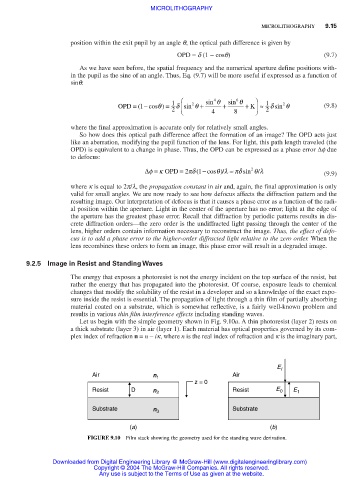
Let us begin with the simple geometry shown in Fig. 9.10a. A thin photoresist (layer 2) rests on
a thick substrate (layer 3) in air (layer 1). Each material has optical properties governed by its com-
plex index of refraction n = n − ik, where n is the real index of refraction and k is the imaginary part,
E I
Air n 1 Air
z = 0
Resist D n 2 Resist E 0 E 1
Substrate n 3 Substrate
(a) (b)
FIGURE 9.10 Film stack showing the geometry used for the standing wave derivation.
Downloaded from Digital Engineering Library @ McGraw-Hill (www.digitalengineeringlibrary.com)
Copyright © 2004 The McGraw-Hill Companies. All rights reserved.
Any use is subject to the Terms of Use as given at the website.