
Page 123 - Semiconductor Manufacturing Handbook
P. 123
Geng(SMH)_CH09.qxd 04/04/2005 19:42 Page 9.22
MICROLITHOGRAPHY
9.22 WAFER PROCESSING
100.
n = 16
80.
Development rate (nm/s) 60. n = 2
40.
20.
0.
.00 .20 .40 .60 .80 1.00
Relative PAC concentration m
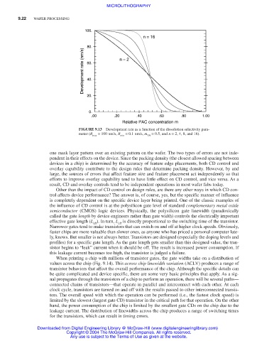
FIGURE 9.13 Development rate as a function of the dissolution selectivity para-
meter (R = 100 nm/s, R = 0.1 nm/s, m = 0.5, and n = 2, 4, 8, and 16).
max min TH
one mask layer pattern over an existing pattern on the wafer. The two types of errors are not inde-
pendent in their effects on the device. Since the packing density (the closest allowed spacing between
devices in a chip) is determined by the accuracy of feature edge placements, both CD control and
overlay capability contribute to the design rules that determine packing density. However, by and
large, the sources of errors that affect feature size and feature placement act independently so that
efforts to improve overlay capability tend to have little effect on CD control, and vice versa. As a
result, CD and overlay controls tend to be independent operations in most wafer fabs today.
Other than the impact of CD control on design rules, are there any other ways in which CD con-
trol affects device performance? The answer is, of course, yes, but the specific manner of influence
is completely dependent on the specific device layer being printed. One of the classic examples of
the influence of CD control is at the polysilicon gate level of standard complementary metal oxide
semiconductor (CMOS) logic devices. Physically, the polysilicon gate linewidth (paradoxically
called the gate length by device engineers rather than gate width) controls the electrically important
effective gate length (L ). In turn, L is directly proportional to the switching time of the transistor.
eff eff
Narrower gates tend to make transistors that can switch on and off at higher clock speeds. Obviously,
faster chips are more valuable than slower ones, as anyone who has priced a personal computer late-
ly, knows. But smaller is not always better. Transistors are designed (especially the doping levels and
profiles) for a specific gate length. As the gate length gets smaller than this designed value, the tran-
sistor begins to “leak” current when it should be off. The result is increased power consumption. If
this leakage current becomes too high, the transistor is judged a failure.
When printing a chip with millions of transistor gates, the gate widths take on a distribution of
values across the chip (Fig. 9.14). This across chip linewidth variation (ACLV) produces a range of
transistor behaviors that affect the overall performance of the chip. Although the specific details can
be quite complicated and device specific, there are some very basic principles that apply. As a sig-
nal propagates through the transistors of a chip to perform an operation, there will be several paths—
connected chains of transistors—that operate in parallel and interconnect with each other. At each
clock cycle, transistors are turned on and off with the results passed to other interconnected transis-
tors. The overall speed with which the operation can be performed (i.e., the fastest clock speed) is
limited by the slowest (largest gate CD) transistor in the critical path for that operation. On the other
hand, the power consumption of the chip is limited by the smallest gate CDs on the chip due to the
leakage current. The distribution of linewidths across the chip produces a range of switching times
for the transistors, which can result in timing errors.
Downloaded from Digital Engineering Library @ McGraw-Hill (www.digitalengineeringlibrary.com)
Copyright © 2004 The McGraw-Hill Companies. All rights reserved.
Any use is subject to the Terms of Use as given at the website.