
Page 148 - Semiconductor Manufacturing Handbook
P. 148
Geng(SMH)_CH11.qxd 04/04/2005 19:48 Page 11.5
WET ETCHING
WET ETCHING 11.5
disordered high-κ films including Hf and Zr sili-
5
cates. Other new HF-based solvent chemistries have 1. Isotropic etch
6
also shown promise. Work is underway to etch the
crystalline form of these high-κ materials and 2. Anisotropic etch
improve the etch selectivity over SiO . In the end,
2
the final solution to the etch challenge will be depen-
dent on the nature of the selected high-κ material,
film deposition method, and optimization of electri- FIGURE 11.7 A wineglass-shaped contact
cal parameters. formed by slope etch followed by straight etch.
11.3 METAL ETCHING
The etching solution for Al is usually a mixture of phosphoric acid (H PO ), acetic acid, and nitric
3 4
acid (HNO ). It is often necessary to conduct the etch at elevated temperatures (approximately 50°C)
3
to dissolve residues. Persulphates, various ammonia mixtures, and dilute sulfuric-acid-peroxide mix-
tures can be used to etch copper. For gold etching, cyanide-based chemistries have been used. Various
other etchant solutions can be used to etch gold, nickel, platinum, chromium, and titanium (Ti).
Even though the isotropic nature of wet etching limits its use in approximately µm level structures,
it still finds use where the feature size is large enough that the undercutting is not a major concern. One
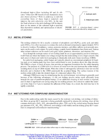
such area is in back-end wafer-level packaging to chemically etch under-bump metallurgy (UBM).
In wafer-level packaging, solder bumps are typically placed on conventional peripheral Al bond-
ing pads or on landing pads that have been redistributed to new locations above the chip circuitry.
The UBM is a layer, or stack of layers, that provides an important foundation for the solder-bumping
process. The purpose of a UBM etch is to remove all metal from the area between the solder bumps,
isolating them on top of UBM islands. When the solder is subsequently reflowed, it does not wet the
dielectric and is limited to the UBM underneath the as-plated bump. The surface tension of the
molten solder pulls it into the desired shape of a truncated sphere (Fig. 11.8).
Although UBM layers may be etched using the dry etch technique, wet etching is generally used
because of the following advantages: (1) the wet etching process etches more efficiently from
beneath the caps of mushroom-plated bumps, (2) no additional cleaning of etch residue is required,
and (3) there is significant cost saving using the wet etching process. It is critical to control the under-
cut to less than 2 to 5 µm to maintain the adhesion of the bump. As a result, the etch time has to be
tightly controlled.
11.4 WET ETCHING FOR COMPOUND SEMICONDUCTOR
Due to the undercutting under the mask caused by the isotropic wet etching, wet etching of dielec-
tric films on group III-V materials is being gradually replaced by plasma dry etching, since all the
common dielectrics (SiO , SiN , phosphosilicate glass, TiN) can be dry etched using fluorine-based
2
x
gas mixtures (CF , SF , NF ). However, wet etching is still widely used in etching group III-V mate-
4
3
6
rials in compound semiconductor manufacturing. 7
Solder UBM etch Solder reflow
UBM
Landing pad
FIGURE 11.8 UBM etch and solder reflow steps in solder-bumping process.
Downloaded from Digital Engineering Library @ McGraw-Hill (www.digitalengineeringlibrary.com)
Copyright © 2004 The McGraw-Hill Companies. All rights reserved.
Any use is subject to the Terms of Use as given at the website.