
Page 172 - Semiconductor Manufacturing Handbook
P. 172
Geng(SMH)_CH12.qxd 04/04/2005 19:49 Page 12.21
PLASMA ETCHING
PLASMA ETCHING 12.21
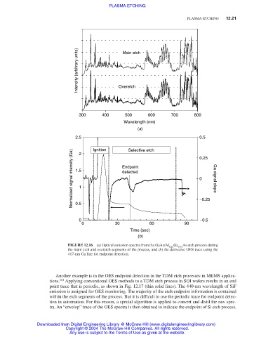
Intensity (arbitrary units) Overetch
Main etch
300 400 500 600 700 800
Wavelength (nm)
(a)
2.5 Ignition Selective etch 0.5
Normalized signal intensity (Ga) 1.5 Endpoint 0.25 Ga signal slope
2
detected
0
1
0.5
0 −0.25
−0.5
0 30 60 90
Time (sec)
(b)
FIGURE 12.16 (a) Optical emission spectra from the GaAs/Al Ga As etch process during
0.25 0.75
the main etch and overetch segments of the process, and (b) the derivative OES trace using the
417-nm Ga line for endpoint detection.
Another example is in the OES endpoint detection in the TDM etch processes in MEMS applica-
tions. 102 Applying conventional OES methods to a TDM etch process in SOI wafers results in an end
point trace that is periodic, as shown in Fig. 12.17 (thin solid lines). The 440-nm wavelength of SiF
emission is assigned for OES monitoring. The majority of the etch endpoint information is contained
within the etch segments of the process. But it is difficult to use the periodic trace for endpoint detec-
tion in automation. For this reason, a special algorithm is applied to convert and distil the raw spec-
tra. An “envelop” trace of the OES spectra is then obtained to indicate the endpoint of Si etch process.
Downloaded from Digital Engineering Library @ McGraw-Hill (www.digitalengineeringlibrary.com)
Copyright © 2004 The McGraw-Hill Companies. All rights reserved.
Any use is subject to the Terms of Use as given at the website.