
Page 167 - Semiconductor Manufacturing Handbook
P. 167
Geng(SMH)_CH12.qxd 04/04/2005 19:49 Page 12.16
PLASMA ETCHING
12.16 WAFER PROCESSING
drift velocity for electrons in GaAs than in Si allow GaAs devices to operate at higher frequencies.
Unlike Si, GaAs is a direct band-gap semiconductor and thus useful for fabricating optical devices.
In etching III-V compound semiconductors, the same set of principles in silicon etching still hold
true. Yet beyond the requirements of etch rate, selectivity, uniformity, and damage control, care must
be taken to maintain chemical stoichiometry at the etched surface while etching III-V materials. 78,79
Here the strategy is again to control the ion-driven and chemical-driven components to achieve the
required balance. Thus, many plasma etching processes require independent controls of plasma den-
sity and bias to make such controls possible.
This chapter will only focus on plasma etching of generic GaAs, InP, and GaN materials. III-V com-
pound semiconductors are typically etched using halogen-based chemistries. Since the group III fluo-
rides (i.e., GaF ) are involatile, most III-V etching is performed using chlorine-, bromine-, or iodine-based
3
chemistries. Other chemistries, such as CH , are also used to etch III-V materials. Table 12.4 provides
4
some common gases used for plasma etching of III-V materials.
12.4.1 Etching of GaAs and Related Materials
Front Etch of GaAs and Related Materials. Front etch of GaAs-based materials (including GaAs,
AlGaAs, and GaSb) is used in making high electron mobility transistors (HEMTs) and heterojunc-
tion bipolar transistors (HBTs). To etch GaAs, chlorine-based chemistry is often employed follow-
ing an ion-enhanced chemical etching mechanism. The addition of oxygen scavengers, such as BCl
3
or SiCl , to the process gas mixture is often necessitated by the difficulty in initiating the GaAs etch-
4
80
ing process in Cl plasma. BCl and PCl gases are often added to Cl when etching AlGaAs mate-
2 3 3 2
rials. BCl and PCl have the ability to getter water vapor in the process chamber as well as attack
3 3
aluminum oxide as it forms.
The chemical reaction taking place is described as
GaAs + 3 Cl ↑= GaCl ↑+ AsCl ↑
2 3 3
However, the group V etch products (AsCl ) have a higher vapor pressure than the group III etch
3
products (GaCl ). This volatility difference makes the removal of the group III (Ga) component in
3
the material rate-limiting, and often results in rough post-etch morphologies and changed chemical
stoichiometry. However, the volatility difference between AsCl and GaCl can be compensated by
3 3
shifting the etch process from a chemical to a more physical regime and controlling substrate tem-
perature. High-energy ion bombardments during etching helps equalize the removal rates in the dif-
ferent crystallographic planes thus resulting in smooth post-etch surface morphologies. Along the
same line, when equirate and step-free etching is required in etching GaAs/AlGaAs device het-
erostructures, adjusting the chemical etching and ion-driven etching components, a balance can be
reached so that the equirate is achieved.
The other prominent issues are related to selectivity and damage control. For example, etching of
GaAs over an AlGaAs etch stop is a key process in the fabrication of high-speed devices. In capacitively
coupled 13.56 MHz RIE plasma processes, selectivity to the underlying AlGaAs etch stop was achieved
81
through the addition of oxygen or fluorine to form nonvolatile AlF . However, the high ion energies
3
associated with the self-induced dc bias at 13.56 MHz results in device damage and compromises
device performance. An alternative option is to use high-density plasma processes in inductively
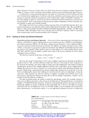
TABLE 12.4 Common Gases Used for Plasma Etching of
III-V Semiconductors
Cl-based Cl , HCl, BCl , CCl , SiCl , PCl , ICl, CCl F
2 3 4 4 3 2
Br-based Br , HBr, CF Br, IBr, HBr/N
2 3 2
I-based HI, I , CH I, ICl
2 3
CH -based CH /H , CH /He, C H /H
4 4 2 4 2 6 2
Downloaded from Digital Engineering Library @ McGraw-Hill (www.digitalengineeringlibrary.com)
Copyright © 2004 The McGraw-Hill Companies. All rights reserved.
Any use is subject to the Terms of Use as given at the website.