
Page 166 - Semiconductor Manufacturing Handbook
P. 166
Geng(SMH)_CH12.qxd 04/04/2005 19:49 Page 12.15
PLASMA ETCHING
PLASMA ETCHING 12.15
+ + + +
Mask Mask
− − − −
− − − −
− − − −
Si
Si Si
Notch
+ + + + + + + +
SiO 2
Insulator Insulator
(a) (b) (c)
FIGURE 12.12 (a) Notching at the Si/oxide interface in a conventional TDM etch process, (b) current
flow within the Si substrate prevents charge separation during bulk etch, and (c) charging effects cause
notching to occur in the overetch period.
high-aspect-ratio structures. At an aspect ratio of 18:1, the notch size is <100 nm for 25 percent
overetch; at aspect ratios exceeding 8:1, no notch is observed for significant overetch up to 50 percent.
12.4 PLASMA ETCHING IN III-V COMPOUND
SEMICONDUCTORS
III-V semiconductors are composed of an element from Column III of the periodic chart and an ele-
ment from Column V of the chart. Indeed, III-V compound semiconductors encompass a variety of
materials. Perhaps the best studied compound semiconductor is GaAs. Compared with Si, compound
semiconductors have some technical advantages. For example, the higher mobility and saturated
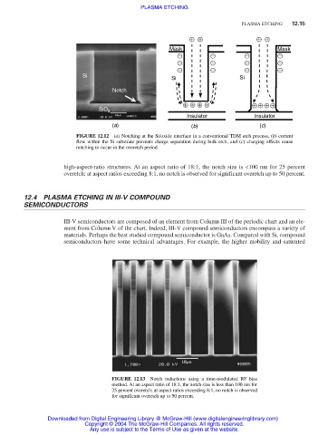
FIGURE 12.13 Notch reductions using a time-modulated RF bias
method. At an aspect ratio of 18:1, the notch size is less than 100 nm for
25 percent overetch; at aspect ratios exceeding 8:1, no notch is observed
for significant overetch up to 50 percent.
Downloaded from Digital Engineering Library @ McGraw-Hill (www.digitalengineeringlibrary.com)
Copyright © 2004 The McGraw-Hill Companies. All rights reserved.
Any use is subject to the Terms of Use as given at the website.