
Page 169 - Semiconductor Manufacturing Handbook
P. 169
Geng(SMH)_CH12.qxd 04/04/2005 19:49 Page 12.18
PLASMA ETCHING
12.18 WAFER PROCESSING
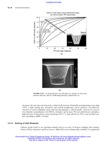
GaAs via wall slope versus photoresist slope
(at various GaAs: PR selectivities)
90 32 16 8
GaAs via wall angle (degrees) 60 (GaAs: PR) 4 2 1 Resist
75
Selectivity
45
30
15
0 GaAs
0 15 30 45 60 75 90
PR wall angle (degrees)
(a)
(b)
FIGURE 12.14 (a) Expected GaAs via wall angle as a function of resist slope
and etch selectivity, and (b) a SEM image showing a sloped GaAs via.
increases, the etch rate and selectivity to hard mask increase. Generally, at temperatures more than
150°C, a high etching rate, selectivity, and smooth morphology can be achieved. The HBr/CH
4
chemistry is used to minimize mask undercut and maintain a vertical profile. And out of concerns
over chamber contamination, the HBr/N chemistry can be used. The etch performance includes a
2
high etch rate (2.0 µm/min), good anisotropy (90 ± 1°), high selectivity (30:1), and excellent sur-
face smoothness (RMS <2.0 nm).
12.4.3 Etching of GaN Materials
Gallium nitride (GaN) is an important material used in an array of devices including light emitting
diodes (LEDs), transistors, and laser devices. Bulk GaN is not commercially available, it is epitaxially
Downloaded from Digital Engineering Library @ McGraw-Hill (www.digitalengineeringlibrary.com)
Copyright © 2004 The McGraw-Hill Companies. All rights reserved.
Any use is subject to the Terms of Use as given at the website.